TMS320TCI6487
TMS320TCI6488
Communications Infrastructure Digital Signal Processor
www.ti.com
SPRS358F–APRIL 2007–REVISED AUGUST 2008
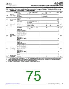
7.3 Electrical Characteristics Over Recommended Ranges of Supply Voltage and Operating
Case Temperature (Unless Otherwise Noted)
PARAMETER
TEST CONDITIONS(1)
MIN
DVDD18 - 0.45
1.4
TYP
MAX UNIT
LVCMOS
IO = IOH
High-level
VOH
DDR2
V
output voltage
I2C/VCNTL
LVCMOS
DDR2
0.1 * DVdd18
IO = IOL
0.45
Low-level output
voltage
VOL
0.4
0.4
5
V
I2C/VCNTL
IO = 3 mA, pulled up to 1.8 V
No IPD/IPU
-5
-169
49
LVCMOS
Internal pullup
-100
100
-47
160
µA
µA
Input current
[DC]
(2)
II
Internal pulldown
0.1 * DVDD18 V < VI < 0.9 *
DVDD18
I2C/VCNTL
-20
20
-8
V
EMU[18:00],
GPIO[15:0], TIMO[1:0]
SYSCLKOUT, TDO,
CLKR0, CLKX0, DX0,
FSR0, FSX0, CLKR1,
CLKX1, DX1, FSR1,
FSX1
-6
High-level
output current
[DC]
IOH
mA
RESETSTAT,
SMFRAMECLK, MDIO,
MDCLK
-4
DDR2
4
8
EMU[18:00],
GPIO[15:0], TIM[1:0]
SYSCLKOUT, TDO,
CLKR0, CLKX0, DX0,
FSR0, FSX0, CLKR1,
CLKX1, DX1, FSR1,
FSX1
6
Low-level output
current [DC]
IOL
mA
RESETSTAT,
SMFRAMECLK, MDIO,
MDCLK
4
DDR2
-4
Off-state output
current [DC]
(3)
IOZ
LVCMOS
-20
20
µA
(1) For test conditions shown as MIN, MAX, or TYP, use the appropriate value specified in the recommended operating conditions table.
(2) II applies to input-only pins and bi-directional pins. For input-only pins, II indicates the input leakage current. For bi-directional pins, II
includes input leakage current and off-state (hi-Z) output leakage current.
(3) IOZ applies to output-only pins, indicating off-state (hi-Z) output leakage current.
Submit Documentation Feedback
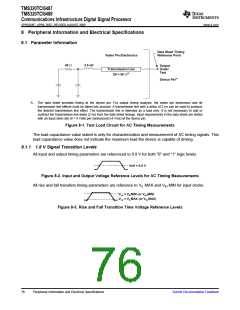
Device Operating Conditions
75

 TI [ TEXAS INSTRUMENTS ]