TMS320TCI6487
TMS320TCI6488
Communications Infrastructure Digital Signal Processor
www.ti.com
SPRS358F–APRIL 2007–REVISED AUGUST 2008
7 Device Operating Conditions
Based
on
JESD22-C101C
(Field-Induced
Charged-Device
Model
Test
Method
for
Electrostatic-Discharge-Withstand Thresholds of Microelectronic Components), the TMS320TCI6487/8
device's charged-device model (CDM) sensitivity classification is Class II (200 to <500 V). Specifically,
DDR memory interface and SERDES pins conform to ±200-V level. All other pins conform to ±500 V.
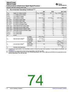
7.1 Absolute Maximum Ratings Over Operating Case Temperature Range (Unless
Otherwise Noted)(1)
CVDD
-0.3 V - 1.35 V
-0.3 V to 1.35 V
DVDD11
DVDD18
-0.3 V to 2.45 V
VREFSSTL
0.49 * DVDD18 to 0.51 * DVDD18
-0.3 V to 1.35 V
AIF_VDDA11, AIF_VDDD11, AIF_VDDT11
Supply voltage range(2)
:
AIF_VDDR18
-0.3 V to 2.45 V
SGR_VDD11, SGR_VDDD11, SGR_VDDT11
-0.3 V to 1.35 V
SGR_VDDR18
AVDD118, AVDD218
VSS Ground
LVCMOS
DDR2
-0.3 V to 2.45 V
-0.3 V to 2.45 V
0 V
-0.3 V to DVDD18 + 0.3 V
-0.3 V to 2.45 V
I2C/VCNTL
LVDS
-0.3 V to 2.45 V
Input voltage (VI) range:
-0.3 V to DVDD18 + 0.3 V
-0.3 V to 1.35 V
LJCB
SERDES
LVCMOS
DDR2
-0.3 V to DVDD11 + 0.3 V
-0.3 V to DVDD18 + 0.3 V
-0.3 V to 2.45 V
Output voltage (VO) range:
I2C/VCNTL
SERDES
-0.3 V to 2.45 V
-0.3 V to DVDD11 + 0.3 V
0°C to 100°C(3)
Operating case temperature range, TC:
Storage temperature range, Tstg
:
-65°C to 150°C
(1) Stresses beyond those listed under "absolute maximum ratings" may cause permanent damage to the device. These are stress ratings
only, and functional operation of the device at these or any other conditions beyond those indicated under "recommended operating
conditions" is not implied. Exposure to absolute-maximum-rated conditions for extended periods may affect device reliability.
(2) All voltage values are with respect to VSS.
(3) A heatsink is required for proper device operation.
Submit Documentation Feedback
Device Operating Conditions
73

 TI [ TEXAS INSTRUMENTS ]