TMS320TCI6487
TMS320TCI6488
Communications Infrastructure Digital Signal Processor
www.ti.com
31
SPRS358F–APRIL 2007–REVISED AUGUST 2008
30
29
28
27
26
25
24
23
22
21
20
19
18
17
16
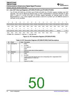
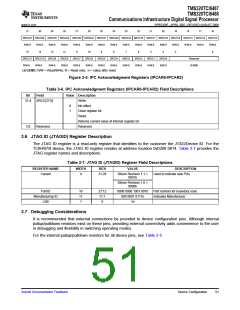
SRCC27 SRCC26 SRCC25 SRCC24 SRCC23 SRCC22 SRCC21 SRCC20 SRCC19 SRCC18 SRCC17 SRCC16 SRCC15 SRCC14 SRCC13 SRCC12
R/W-0
15
R/W-0
14
R/W-0
R/W-0
R/W-0
R/W-0
R/W-0
R/W-0
R/W-0
R/W-0
R/W-0
R/W-0
R/W-0
3
R/W-0
R/W-0
R/W-0
0
13
12
11
10
9
8
7
6
5
4
SRCC11 SRCC10
R/W-0 R/W-0
SRCC9
R/W-0
SRCC8
R/W-0
SRCC7
R/W-0
SRCC6
R/W-0
SRCC5
R/W-0
SRCC4
R/W-0
SRCC3
R/W-0
SRCC2
R/W-0
SRCC1
R/W-0
SRCC0
R/W-0
Reserved
R-0000
LEGEND: R/W = Read/Write; R = Read only; -n = value after reset
Figure 3-3. IPC Acknowledgment Registers (IPCAR0-IPCAR2)
Table 3-6. IPC Acknowledgment Registers (IPCAR0-IPCAR2) Field Descriptions
Bit
Field
Value Description
31:4
SRCC[27:0]
Write:
0
1
No effect
Clear register bit
Read:
Returns current value of internal register bit
Reserved
3:0
Reserved
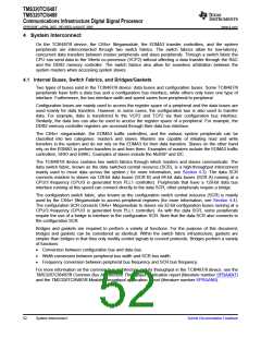
3.6 JTAG ID (JTAGID) Register Description
The JTAG ID register is a read-only register that identifies to the customer the JTAG/Device ID. For the
TCI6487/8 device, the JTAG ID register resides at address location 0x0288 0814. Table 3-7 provides the
JTAG register names and descriptions.
Table 3-7. JTAG ID (JTAGID) Register Field Descriptions
REGISTER NAME
WIDTH
BITS
VALUE
DESCRIPTION
Used to indicate new PGs
Variant
4
31:28
Silicon Revision 1.1 =
0001b
Silicon Revision 1.0 =
0000b
PartID
Manufacturing ID
LSB
16
11
1
27:12
11:1
0
0000 0000 1001 0010
000 0001 0111b
1b
Part number for boundary scan.
Indicates Manufacturer
3.7 Debugging Considerations
It is recommended that external connections be provided to device configuration pins. Although internal
pullup/pulldown resistors exist on these pins, providing external connectivity adds convenience to the user
in debugging and flexibility in switching operating modes.
For the internal pullup/pulldown resistors for all device pins, see Table 2-5.
Submit Documentation Feedback
Device Configuration
51

 TI [ TEXAS INSTRUMENTS ]