TMS320TCI6487
TMS320TCI6488
Communications Infrastructure Digital Signal Processor
SPRS358F–APRIL 2007–REVISED AUGUST 2008
www.ti.com
3.4 Device Status Register Descriptions
The device status register depicts the device configuration selected upon device reset. Once set, these
bits remain set until a device reset.
Table 3-3 shows the parameters that are set through software to configure different components on the
device. The configuration is done through the device configuration DEVCFG register, which is one-time
writeable through software. The register is reset on all hard resets and is locked after the first write.
Table 3-3. Device Configuration Register Fields
FIELD
RESET
DESCRIPTION
SETTINGS
Device Configuration 1 Register Fields
McBSP0 CLKS Select 0: CLKS0 device pin
CLKS0
CLKS1
0b
0b
1b
1: chip_clks from Main.PLL
McBSP1 CLKS Select
SYSCLKOUT Enable
0: CLKS1 device pin
1: chip_clks from Main.PLL
SYSCLKOUTEN
0: No Clock Output
1: Clock output Enabled
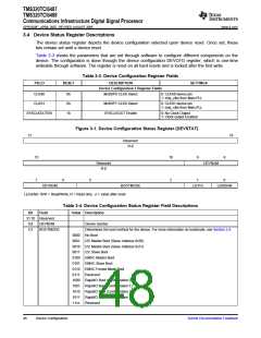
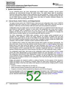
Figure 3-1. Device Configuration Status Register (DEVSTAT)
31
15
7
16
Reserved
R-0
10
2
9
8
0
Reserved
R-0
DEVNUM
6
5
1
DEVNUM
BOOTMODE
L2CFG
LENDIAN
LEGEND: R/W = Read/Write; R = Read only; -n = value after reset
Table 3-4. Device Configuration Status Register Field Descriptions
Bit
Field
Value Description
31:10 Reserved
9:6
5:2
DEVNUM
Device number
BOOTMODE
Determines the boot method for the device. For more information on bootmode, see Section 2.4.
0000 No Boot
0001 I2C Master Boot (Slave Address 0x50)
0010 I2C Master Boot (Slave Address 0x51)
0011 I2C Slave Boot
0100 EMAC Master Boot
0101 EMAC Slave Boot
0110 EMAC Forced Mode Boot
0111 Reserved
1000 RapidIO Boot (Configuration 0)
1001 RapidIO Boot (Configuration 1)
1010 RapidIO Boot (Configuration 2)
1011 RapidIO Boot (Configuration 3)
11xx
Reserved
48
Device Configuration
Submit Documentation Feedback

 TI [ TEXAS INSTRUMENTS ]