TMS320TCI6487
TMS320TCI6488
Communications Infrastructure Digital Signal Processor
SPRS358F–APRIL 2007–REVISED AUGUST 2008
www.ti.com
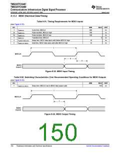
8.13.2 MDIO Electrical Data/Timing
Table 8-51. Timing Requirements for MDIO Inputs
(see Figure 8-32)
NO.
MIN
400
180
180
MAX UNIT
1
2a
2b
3
tc(MDCLK)
Cycle time, MDCLK
ns
ns
ns
tw(MDCLK)
Pulse duration, MDCLK high
tw(MDCLK)
Pulse duration, MDCLK low
tt(MDCLK)
Transition time, MDCLK
5
ns
ns
ns
4
tsu(MDIO-MDCLKH)
th(MDCLKH-MDIO)
Setup time, MDIO data input valid before MDCLK high
Hold time, MDIO data input valid after MDCLK high
10
10
5
1
MDCLK
4
5
MDIO
(input)
Figure 8-32. MDIO Input Timing
Table 8-52. Switching Characteristics Over Recommended Operating Conditions for MDIO Outputs
(see Figure 8-33)
NO.
MIN
MAX UNIT
100 ns
7
td(MDCLKL-MDIO)
Delay time, MDCLK low to MDIO data output valid
1
MDCLK
7
MDIO
(input)
Figure 8-33. MDIO Output Timing
150
Peripheral Information and Electrical Specifications
Submit Documentation Feedback

 TI [ TEXAS INSTRUMENTS ]