TMS320TCI6487
TMS320TCI6488
Communications Infrastructure Digital Signal Processor
SPRS358F–APRIL 2007–REVISED AUGUST 2008
www.ti.com
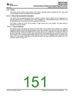
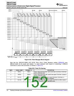
FSEVT2
TIMI0
TIMI1
SYSCLK/6
TIMO0
TIMO1
FSEVT3
TINPHSEL 0
TINPLSEL 0
TINPHSEL 1
TINPLSEL 1
TINPHSEL 2
TINPLSEL 2
TINPHSEL 3
TINPLSEL 3
TINPHSEL 4
TINPLSEL 4
TINPHSEL 5
TINPLSEL 5
TOUTSEL 1
TOUTSEL 0
0 1 2 3
0 1 2 3
0 1 2 3
0 1 2 3
0 1 2 3
0 1 2 3
0 1 2 3
0 1 2 3
0 1 2 3
0 1 2 3
0 1 2 3
0 1 2 3
0 1 2 3 4 5 6 7 8 91011
0 1 2 3 4 5 6 7 8 91011
Timer Pin Manager
(TPMGR)
Timer64
Timer64
Timer642
Timer64
Timer64
Timer64
0
1
2
3
4
5
32
CFG SCR
(SCR F)
vbusp
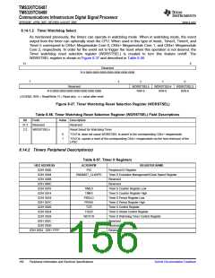
Figure 8-34. Timer Manager Block Diagram
Note that the TMS320TCI648x DSP 64-Bit Timer User’s Guide (literature number SPRU818) uses
different labels for its inputs and outputs. To avoid confusion with respect to numbering, a different
convention is used in this document, as shown in Table 8-53.
Table 8-53. Timer Pin Naming
TIMER
SIGNAL NAME
RENAMED TO
DESCRIPTION
n
TINP12
TINPLn
Timer n input event (low half). Used to drive lower 32-bit timer, 64-bit timer.
Used in watchdog mode.
n
n
n
TINP34
TOUT12
TOUT34
TINPHn
TOUTLn
TOUTHn
Timer n input event (high half). Used to drive upper 32-bit timer. Unused in
64-bit or watchdog modes.
Timer n output (low half). Driven by lower 32-bit timer, 64-bit timer, or
watchdog timer as either a pulse or waveform.
Timer n output (high half). Driven by upper 32-bit timer as either a pulse or
waveform. Unused in 64-bit or watchdog modes.
152
Peripheral Information and Electrical Specifications
Submit Documentation Feedback

 TI [ TEXAS INSTRUMENTS ]