TMS320TCI6487
TMS320TCI6488
Communications Infrastructure Digital Signal Processor
www.ti.com
SPRS358F–APRIL 2007–REVISED AUGUST 2008
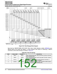
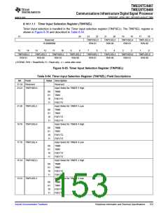
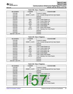
8.14.1.1.1 Timer Input Selection Register (TINPSEL)
Timer input selection is handled in the Timer input selection register (TINPSEL). The TINPSEL register is
shown in Figure 8-35 and described in Table 8-54.
31
15
24
23
22
21
20
19
18
17
16
Reserved
TINPHSEL5
R/W-01
TINPLSEL5
R/W-00
TINPHSEL4
R/W-01
TINPLSEL4
R/W-00
R-00000000
14
13
12
11
10
9
8
7
6
5
4
3
2
1
0
TINPHSEL3
R/W-01
TINPLSEL3
R/W-00
TINPHSEL2
R/W-01
TINPLSEL2
R/W-00
TINPHSEL1
R/W-01
TINPLSEL1
R/W-00
TINPHSEL0
R/W-01
TINPLSEL0
R/W-00
LEGEND: R/W = Read/Write; R = Read only; -n = value after reset
Figure 8-35. Timer Input Selection Register (TINPSEL)
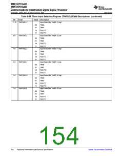
Table 8-54. Timer Input Selection Register (TINPSEL) Field Descriptions
Bit
Field
Value Description
Reserved
31-24 Reserved
23:22 TINPHSEL5
Input Select for TIMER 5 High
00
01
10
11
TIMI0
TIMI1
FSEVT2
FSEVT3
21:20 TINPLSEL5
19:18 TINPHSEL4
17:16 TINPLSEL4
15:14 TINPHSEL3
13:12 TINPLSEL3
Input Select for TIMER 5 Low
00
01
10
11
TIMI0
TIMI1
FSEVT2
FSEVT3
Input Select for TIMER 4 High
00
01
10
11
TIMI0
TIMI1
FSEVT2
FSEVT3
Input Select for TIMER 4 Low
00
01
10
11
TIMI0
TIMI1
FSEVT2
FSEVT3
Input Select for TIMER 3 High
00
01
10
11
TIMI0
TIMI1
FSEVT2
FSEVT3
Input Select for TIMER 3 Low
00
01
10
11
TIMI0
TIMI1
FSEVT2
FSEVT3
Submit Documentation Feedback
Peripheral Information and Electrical Specifications
153

 TI [ TEXAS INSTRUMENTS ]