TMS320TCI6487
TMS320TCI6488
Communications Infrastructure Digital Signal Processor
SPRS358F–APRIL 2007–REVISED AUGUST 2008
www.ti.com
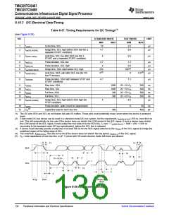
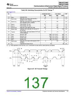
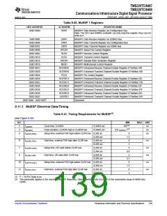
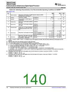
Table 8-42. Switching Characteristics Over Recommended Operating Conditions for McBSP(1)(2)
(see Figure 8-28)
NO.
MIN
MAX UNIT
1
td(CKSH-CKRXH)
Delay time, CLKS high to CLKR/X high for internal CLKR/X
generated from CLKS input.(3)
1.4
10
ns
2
3
tc(CKRX)
tw(CKRX)
Cycle time, CLKR/X
CLKR/X int
CLKR/X int
10P(4)
C - 1(5)
ns
ns
Pulse duration, CLKR/X high or
CLKR/X low
C + 1(5)
3
4
9
td(CKRH-FRV)
td(CKXH-FXV)
Delay time, CLKR high to internal CLKR int
FSR valid
-2.1
ns
ns
Delay time, CLKX high to internal CLKX int
FSX valid
-1.7
1.7
3
9
4
9
CLKX ext
12
tdis(CKXH-DXHZ)
Disable time, DX high impedance CLKX int
following last data bit from CLKX
high
-3.9
2.1
ns
ns
CLKX ext
CLKX int
Delay time, CLKX high to DX valid CLKX ext (DXENA = 0)
CLKX ext (DXENA = 1)
-3.9 +D1(6)
2.1(6)
2.1 + D1(6)
-2.3 + D1(7)
1.9 + D1(7)
4 + D2(6)
9(6)
9 + D2(6)
5.6 + D2(7)
9 + D2(7)
13
14
td(CKXH-DXV)
Delay time, FSX high to DX valid
ONLY applies when in data delay
0 (XDATDLY = 00b)mode
FSX int
FSX ext
ns
td(FXH-DXV)
(1) CLKRP = CLKXP = FSRP = FSXP = 0. If polarity of any of the signals is inverted, then the timing references of that signal are also
inverted.
(2) Minimum delay times also represent minimum output hold times.
(3) The CLKS signal is shared by both McBSP0 and McBSP1 on this device.
(4) P = 1/CPU clock frequency, in ns. For example, when running parts at 1000 MHz, use P = 1 ns.
(5) C = H or L S = sample rate generator input clock = 6P if CLKSM = 1 (P = 1/CPU clock frequency)
S = sample rate generator input clock = P_clks if CLKSM = 0 (P_clks = CLKS period)
H = CLKX high pulse width = (CLKGDV/2 + 1) * S if CLKGDV is even
H = (CLKGDV + 1)/2 * S if CLKGDV is odd L = CLKX low pulse width = (CLKGDV/2) * S if CLKGDV is even
L = (CLKGDV + 1)/2 * S if CLKGDV is odd CLKGDV should be set appropriately to ensure the McBSP bit rate does not exceed the
maximum limit (see (4) above).
(6) Extra delay from CLKX high to DX valid applies only to the first data bit of a device, if and only if DXENA = 1 in SPCR.
if DXENA = 0, then D1 = D2 = 0
if DXENA = 1, then D1 = 6P, D2 = 12P
(7) Extra delay from FSX high to DX valid applies only to the first data bit of a device, if and only if DXENA = 1 in SPCR.
if DXENA = 0, then D1 = D2 = 0
if DXENA = 1, then D1 = 6P, D2 = 12P
140
Peripheral Information and Electrical Specifications
Submit Documentation Feedback

 TI [ TEXAS INSTRUMENTS ]