TMS320TCI6487
TMS320TCI6488
Communications Infrastructure Digital Signal Processor
www.ti.com
SPRS358F–APRIL 2007–REVISED AUGUST 2008
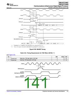
(1)
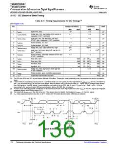
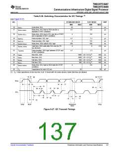
Table 8-38. Switching Characteristics for I2C Timings
(see Figure 8-27)
NO.
STANDARD MODE
MIN MAX
FAST MODE
UNIT
MIN
2.5
MAX
16
17
tc(SCL)
Cycle time, SCL
10
µs
µs
td(SCLH-SDAL)
Delay time, SCL high to SDA low (for a
repeated START condition)
4.7
0.6
18
td(SDAL-SCLL)
Delay time, SDA low to SCL low (for a START
and a repeated START condition)
4
0.6
µs
19
20
21
22
tw(SCLL)
Pulse duration, SCL low
4.7
4
1.3
0.6
100
0
µs
µs
ns
µs
tw(SCLH)
Pulse duration, SCL high
td(SDAV-SDLH)
ttw(SDLL-SDAV)
Delay time, SDA valid to SCL high
250
0
Valid time, SDA valid after SCL low (for PC
bus devices)
0.9
23
Tw(SDAH)
Pulse duration, SDA high between STOP and
START conditions
4.7
1.3
µs
(1)
24
25
26
27
28
tr(SDA)
Rise time, SDA
Rise time, SCL
Fall time, SDA
Fall time, SCL
1000 20 + 0.1Cb
300
300
300
300
ns
ns
ns
ns
µs
(1)
(1)
(1)
tr(SDL)
1000 20 + 0.1Cb
300 20 + 0.1Cb
300 20 + 0.1Cb
tf(SDA)
tf(SCL)
td(SCLH-SDAH)
Delay time, SCL high to SDA high (for STOP
condition)
4
0.6
29
Cp
Capacitance for each I2C pin
10
10
pF
(1) Cb = total capacitance of one bus line, in pF. If mixed with HS-mode devices, faster fall-times are allowed.
Figure 8-27. I2C Transmit Timings
Submit Documentation Feedback
Peripheral Information and Electrical Specifications
137

 TI [ TEXAS INSTRUMENTS ]