TMS320TCI6487
TMS320TCI6488
Communications Infrastructure Digital Signal Processor
www.ti.com
SPRS358F–APRIL 2007–REVISED AUGUST 2008
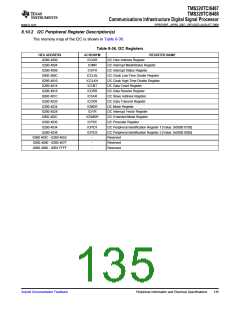
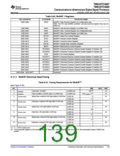
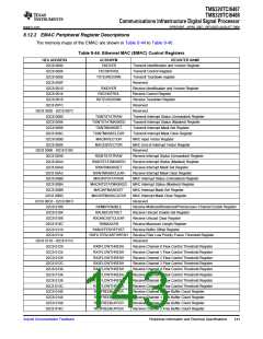
Table 8-40. McBSP 1 Registers
HEX ADDRESS
ACRONYM
REGISTER NAME
028D 0000
DRR1
McBSP1 Data Receive Register via Configuration Bus.
Note: The CPU and EDMA3 controller can only read this register; they can not
write to it.
3400 0000
028D 0004
3400 0010
028D 0008
028D 000C
028D 0010
028D 0014
028D 0018
028D 001C
028D 0020
028D 0024
028D 0028
028D 002C
028D 0030
028D 0034
028D 0038
028D 003C
DRR1
DXR1
McBSP1 Data Receive Register via EDMA3 Bus
McBSP1 Data Transmit Register via Configuration Bus
McBSP1 Data Transmit Register via EDMA Bus
McBSP1 Serial Port Control Register
DXR1
SPCR1
RCR1
McBSP1 Receive Control Register
XCR1
McBSP1 Transmit Control Register
SRGR1
MCR1
McBSP1 Sample Rate Generator Register
McBSP1 Multichannel Control Register
RCERE01
XCERE01
PCR1
McBSP1 Enhanced Receive Channel Enable Register 0 Partition A/B
McBSP1 Enhanced Transmit Channel Enable Register 0 Partition A/B
McBSP1 Pin Control Register
RCERE11
XCERE11
RCERE21
XCERE21
RCERE31
XCERE3
-
McBSP1 Enhanced Receive Channel Enable Register 0 Partition C/D
McBSP1 Enhanced Transmit Channel Enable Register 0 Partition C/D
McBSP1 Enhanced Receive Channel Enable Register 0 Partition E/F
McBSP1 Enhanced Transmit Channel Enable Register 0 Partition E/F
McBSP1 Enhanced Receive Channel Enable Register 0 Partition G/H
McBSP1 Enhanced Transmit Channel Enable Register 0 Partition G/H
Reserved
028D 0040 - 028D 00FF
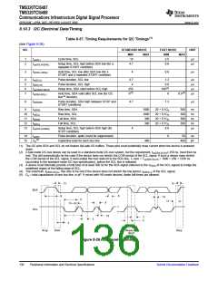
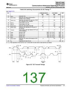
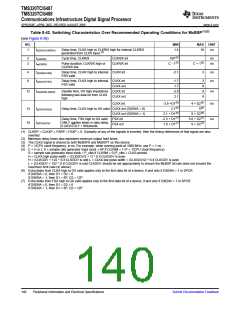
8.11.3 McBSP Electrical Data/Timing
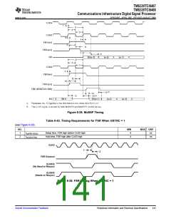
Table 8-41. Timing Requirements for McBSP(1)
(see Figure 8-28)
NO.
MIN
MAX UNIT
2
3
5
tc(CKRX)
Cycle time, CLKR/X
CLKR/X ext
CLKR/X ext
10P(2)
0.5t c(CKRX)-1(2)
ns
ns
ns
tw(CKRX)
Pulse duration, CLKR/X high or CLKR/X low
tsu(FRH-CKRL)
Setup time, external FSR high before CLKR low CLKR int
CLKR ext
9
1.3
6
6
7
th(CKRL-FRH)
tsu(DRV-CKRL)
th(CKRL-DRV)
tsu(FXH-CKXL)
th(CKXL-FXH)
Hold time, external FSR high after CLKR low
Setup time, DR valid before CLKR low
Hold time, DR valid after CLKR low
CLKR int
CLKR ext
CLKR int
CLKR ext
CLKR int
CLKR ext
ns
ns
ns
ns
ns
3
8
0.9
3
8
3.1
9
10
11
Setup time, external FSX high before CLKX low CLKR int
CLKR ext
1.3
6
Hold time, external FSX high after CLKX low
CLKR int
CLKR ext
3
(1) P = 1/CPU Clock in ns.
(2) This parameter applies to the maximum McBSP frequency. Operate serial clocks (CLKR/X) in the reasonable range of 40/60 duty
cycles.
Submit Documentation Feedback
Peripheral Information and Electrical Specifications
139

 TI [ TEXAS INSTRUMENTS ]