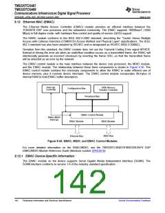
TMS320TCI6487
TMS320TCI6488
Communications Infrastructure Digital Signal Processor
SPRS358F–APRIL 2007–REVISED AUGUST 2008
www.ti.com
8.11 Multichannel Buffered Serial Port (McBSP)
The McBSP provides these functions:
•
•
•
•
Full-duplex communication
Double-buffered data registers, which allow a continuous data stream
Independent framing and clocking for receive and transmit
Direct interface to industry-standard codecs, analog interface chips (AICs), and other serially
connected analog-to-digital (A/D) and digital-to-analog (D/A) devices
•
External shift clock or an internal, programmable frequency shift clock for data transfer
For more detailed information on the McBSP peripheral, see the TMS320TCI648x DSP Multichannel
Buffered Serial Port (McBSP) Reference Guide (literature number SPRU803).
8.11.1 McBSP Device-Specific Information
The CLKS signal for MCBSP0 and MCBSP1 can be sourced from an external pin or by PLL Controller 1.
For details, see Section 8.7. If the clock from the PLL Controller 1 is used, the clock is shared between the
two McBSPs.
8.11.2 McBSP Peripheral Register Descriptions
The memory map of the McBSP 0 registers is shown in Table 8-39.
Table 8-39. McBSP 0 Registers
HEX ADDRESS
ACRONYM
REGISTER NAME
028C 0000
DRR0
McBSP0 Data Receive Register via Configuration Bus.
Note: The CPU and EDMA3 controller can only read this register; they can not
write to it.
3000 0000
028C 0004
DRR0
DXR0
McBSP0 Data Receive Register via EDMA3 Bus
McBSP0 Data Transmit Register via Configuration Bus
McBSP0 Data Transmit register via EDMA bus
3000 0010
DXR0
028C 0008
SPCR0
RCR0
McBSP0 Serial Port Control Register
028C 000C
028C 0010
McBSP0 Receive Control Register
XCR0
McBSP0 Transmit Control Register
028C 0014
SRGR0
MCR0
McBSP0 Sample Rate Generator Register
028C 0018
McBSP0 Multichannel Control Register
028C 001C
028C 0020
RCERE00
XCERE00
PCR0
McBSP0 Enhanced Receive Channel Enable Register 0 Partition A/B
McBSP0 Enhanced Transmit Channel Enable Register 0 Partition A/B
McBSP0 Pin Control Register
028C 0024
028C 0028
RCERE10
XCERE10
RCERE20
XCERE20
RCERE30
XCERE30
-
McBSP0 Enhanced Receive Channel Enable Register 0 Partition C/D
McBSP0 Enhanced Transmit Channel Enable Register 0 Partition C/D
McBSP0 Enhanced Receive Channel Enable Register 0 Partition E/F
McBSP0 Enhanced Transmit Channel Enable Register 0 Partition E/F
McBSP0 Enhanced Receive Channel Enable Register 0 Partition G/H
McBSP0 Enhanced Transmit Channel Enable Register 0 Partition G/H
Reserved
028C 002C
028C 0030
028C 0034
028C 0038
028C 003C
028C 0040 - 028C 00FF
The memory map of the McBSP 1 registers is shown in Table 8-40.
138
Peripheral Information and Electrical Specifications
Submit Documentation Feedback

 TI [ TEXAS INSTRUMENTS ]