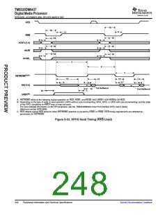
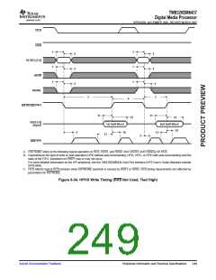
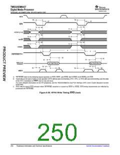
TMS320DM6437
Digital Media Processor
www.ti.com
SPRS345B–NOVEMBER 2006–REVISED MARCH 2007
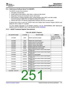
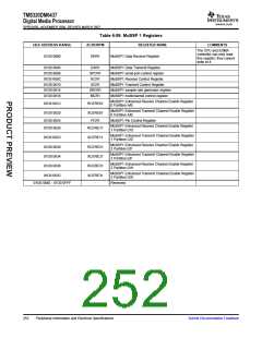
Table 6-59. McBSP 1 Registers
HEX ADDRESS RANGE
ACRONYM
REGISTER NAME
COMMENTS
The CPU and EDMA
controller can only read
this register; they cannot
write to it.
01D0 0800
DRR1
McBSP1 Data Receive Register
01D0 0804
01D0 0808
01D0 080C
01D0 0810
01D0 0814
01D0 0818
DXR1
SPCR1
RCR1
McBSP1 Data Transmit Register
McBSP1 serial port control register
McBSP1 Receive Control Register
McBSP1 Transmit Control Register
McBSP1 sample rate generator register
McBSP1 multichannel control register
XCR1
SRGR1
MCR1
McBSP1 Enhanced Receive Channel Enable Register
0 Partition A/B
01D0 081C
RCERE01
McBSP1 Enhanced Transmit Channel Enable Register
0 Partition A/B
01D0 0820
01D0 0824
01D0 0828
XCERE01
PCR1
McBSP1 Pin Control Register
McBSP1 Enhanced Receive Channel Enable Register
1 Partition C/D
RCERE11
McBSP1 Enhanced Transmit Channel Enable Register
1 Partition C/D
01D0 082C
01D0 0830
01D0 0834
01D0 0838
XCERE11
RCERE21
XCERE21
RCERE31
McBSP1 Enhanced Receive Channel Enable Register
2 Partition E/F
McBSP1 Enhanced Transmit Channel Enable Register
2 Partition E/F
McBSP1 Enhanced Receive Channel Enable Register
3 Partition G/H
McBSP1 Enhanced Transmit Channel Enable Register
3 Partition G/H
01D0 083C
XCERE31
-
01D0 0840 - 01D0 0FFF
Reserved
252
Peripheral Information and Electrical Specifications
Submit Documentation Feedback

 TI [ TEXAS INSTRUMENTS ]