TMS320DM6437
Digital Media Processor
www.ti.com
SPRS345B–NOVEMBER 2006–REVISED MARCH 2007
6.14 Multichannel Buffered Serial Port (McBSP)
The McBSP provides these functions:
•
•
•
•
Full-duplex communication
Double-buffered data registers, which allow a continuous data stream
Independent framing and clocking for receive and transmit
Direct interface to industry-standard codecs, analog interface chips (AICs), and other serially
connected analog-to-digital (A/D) and digital-to-analog (D/A) devices
•
External shift clock or an internal, programmable frequency shift clock for data transfer
If internal clock source is used, the CLKGDV field of the Sample Rate Generator Register (SRGR) must
always be set to a value of 1 or greater.
For more detailed information on the McBSP peripheral, see the TMS320DM643x DMP Multichannel
Buffered Serial Port (McBSP) User's Guide (literature number SPRU943).
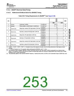
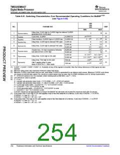
6.14.1 McBSP Peripheral Register Description(s)
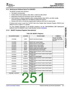
Table 6-58. McBSP 0 Registers
HEX ADDRESS RANGE
ACRONYM
REGISTER NAME
COMMENTS
The CPU and EDMA3
controller can only read
this register; they cannot
write to it.
01D0 0000
DRR0
McBSP0 Data Receive Register
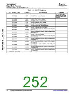
01D0 0004
01D0 0008
01D0 000C
01D0 0010
01D0 0014
01D0 0018
DXR0
SPCR0
RCR0
McBSP0 Data Transmit Register
McBSP0 Serial Port Control Register
McBSP0 Receive Control Register
McBSP0 Transmit Control Register
McBSP0 Sample Rate Generator register
McBSP0 Multichannel Control Register
XCR0
SRGR0
MCR0
McBSP0 Enhanced Receive Channel Enable Register
0 Partition A/B
01D0 001C
RCERE00
McBSP0 Enhanced Transmit Channel Enable Register
0 Partition A/B
01D0 0020
01D0 0024
01D0 0028
XCERE00
PCR0
McBSP0 Pin Control Register
McBSP0 Enhanced Receive Channel Enable Register
1 Partition C/D
RCERE10
McBSP0 Enhanced Transmit Channel Enable Register
1 Partition C/D
01D0 002C
01D0 0030
01D0 0034
01D0 0038
XCERE10
RCERE20
XCERE20
RCERE30
McBSP0 Enhanced Receive Channel Enable Register
2 Partition E/F
McBSP0 Enhanced Transmit Channel Enable Register
2 Partition E/F
McBSP0 Enhanced Receive Channel Enable Register
3 Partition G/H
McBSP0 Enhanced Transmit Channel Enable Register
3 Partition G/H
01D0003C
XCERE30
-
01D0 0040 - 01D0 07FF
Reserved
Submit Documentation Feedback
Peripheral Information and Electrical Specifications
251

 TI [ TEXAS INSTRUMENTS ]