TMS320DM6437
Digital Media Processor
www.ti.com
SPRS345B–NOVEMBER 2006–REVISED MARCH 2007
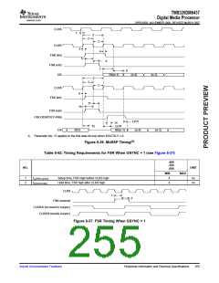
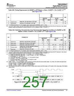
Table 6-63. Timing Requirements for McBSP as SPI Master or Slave: CLKSTP = 10b, CLKXP = 0(1)(2)
(see Figure 6-38)
-400
-500
-600
NO.
UNIT
MASTER
SLAVE
MIN
MIN
14
4
MAX
MAX
4
5
tsu(DRV-CKXL)
th(CKXL-DRV)
Setup time, DR valid before CLKX low
Hold time, DR valid after CLKX low
2 - 3P
5 + 6P
ns
ns
(1) P = SYSCLK3 period in ns. For example, when running parts at 600 MHz, use P = 10 ns.
(2) For all SPI Slave modes, the rate of the internal clock CLKG must be at least 8 times faster than that of the SPI data rate. User should
program sample rate generator to achieve maximum CLKG by setting CLKSM = CLKGDV = 1.
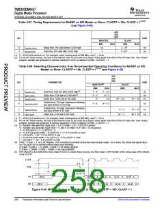
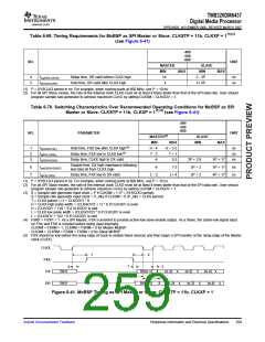
Table 6-64. Switching Characteristics Over Recommended Operating Conditions for McBSP as SPI
Master or Slave: CLKSTP = 10b, CLKXP = 0(1)(2) (see Figure 6-38)
-400
-500
-600
NO.
PARAMETER
UNIT
MASTER(3)
MIN
SLAVE
MIN
MAX
MAX
1
2
3
th(CKXL-FXL)
td(FXL-CKXH)
td(CKXH-DXV)
Hold time, FSX low after CLKX low(4)
Delay time, FSX low to CLKX high(5)
Delay time, CLKX high to DX valid
T - 4
L - 2
-4
T + 5.5
L + 4
5.5
ns
ns
ns
3P + 2.8
5P + 17
Disable time, DX high impedance following
last data bit from CLKX low
6
tdis(CKXL-DXHZ)
L - 6
L + 7.5
ns
Disable time, DX high impedance following
last data bit from FSX high
7
8
tdis(FXH-DXHZ)
td(FXL-DXV)
P + 3
3P + 17
4P + 17
ns
ns
Delay time, FSX low to DX valid
2P + 1.8
(1) P = SYSCLK3 period in ns. For example, when running parts at 600 MHz, use P = 10 ns.
(2) For all SPI Slave modes, the rate of the internal clock CLKG must be at least 8 times faster than that of the SPI data rate. User should
program sample rate generator to achieve maximum CLKG by setting CLKSM = CLKGDV = 1.
(3) S = Sample rate generator input clock = P if CLKSM = 1 (P = SYSCLK3 period)
S = Sample rate generator input clock = P_clks if CLKSM = 0 (P_clks = CLKS period)
T = CLKX period = (1 + CLKGDV) * S
H = CLKX high pulse width = (CLKGDV/2 + 1) * S if CLKGDV is even
H = (CLKGDV + 1)/2 * S if CLKGDV is odd
L = CLKX low pulse width = (CLKGDV/2) * S if CLKGDV is even
L = (CLKGDV + 1)/2 * S if CLKGDV is odd
(4) FSRP = FSXP = 1. As a SPI Master, FSX is inverted to provide active-low slave-enable output. As a Slave, the active-low signal input
on FSX and FSR is inverted before being used internally.
CLKXM = FSXM = 1, CLKRM = FSRM = 0 for Master McBSP
CLKXM = CLKRM = FSXM = FSRM = 0 for Slave McBSP
(5) FSX should be low before the rising edge of clock to enable Slave devices and then begin a SPI transfer at the rising edge of the Master
clock (CLKX).
CLKX
1
2
8
FSX
7
6
3
DX
DR
Bit 0
Bit(n-1)
Bit(n-1)
(n-2)
(n-3)
(n-3)
(n-4)
4
5
Bit 0
(n-2)
(n-4)
Figure 6-38. McBSP Timing as SPI Master or Slave: CLKSTP = 10b, CLKXP = 0
256
Peripheral Information and Electrical Specifications
Submit Documentation Feedback

 TI [ TEXAS INSTRUMENTS ]