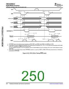
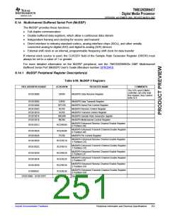
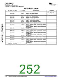
TMS320DM6437
Digital Media Processor
www.ti.com
SPRS345B–NOVEMBER 2006–REVISED MARCH 2007
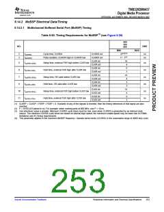
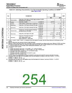
Table 6-61. Switching Characteristics Over Recommended Operating Conditions for McBSP(1)(2)
(see Figure 6-36)
-400
-500
-600
NO.
PARAMETER
UNIT
MIN
MAX
Delay time, CLKS high to CLKR/X high for internal CLKR/X
generated from CLKS input
1
td(CKSH-CKRXH)
3
10
ns
2
3
4
tc(CKRX)
Cycle time, CLKR/X
CLKR/X int
CLKR/X int
CLKR int
CLKX int
CLKX ext
CLKX int
CLKX ext
CLKX int
CLKX ext
FSX int
2P(3)(4)(5)
C - 1(6)
-4
ns
ns
ns
tw(CKRX)
Pulse duration, CLKR/X high or CLKR/X low
Delay time, CLKR high to internal FSR valid
C + 1(6)
5.5
td(CKRH-FRV)
-4
5.5
9
td(CKXH-FXV)
tdis(CKXH-DXHZ)
td(CKXH-DXV)
Delay time, CLKX high to internal FSX valid
ns
ns
ns
2.5
14.5
-5.5
7.5
Disable time, DX high impedance following
last data bit from CLKX high
12
13
-2.1
-4 + D1(7)
2.5 + D1(7) 14.5 + D2(7)
16
5.5 + D2(7)
Delay time, CLKX high to DX valid
Delay time, FSX high to DX valid
-3.9(8)
5(8)
14
td(FXH-DXV)
ns
ONLY applies when in data
delay 0 (XDATDLY = 00b) mode
FSX ext
-2.1(8)
5(8)
(1) CLKRP = CLKXP = FSRP = FSXP = 0. If polarity of any of the signals is inverted, then the timing references of that signal are also
inverted.
(2) Minimum delay times also represent minimum output hold times.
(3) Minimum CLKR/X cycle times must be met, even when CLKR/X is generated by an internal clock source. Minimum CLKR/X cycle times
are based on internal logic speed; the maximum usable speed may be lower due to EDMA limitations and AC timing requirements.
(4) P = SYSCLK3 period in ns. For example, when running parts at 600 MHz, use P = 10 ns.
(5) Use whichever value is greater.
(6) C = H or L
S = sample rate generator input clock = P if CLKSM = 1 (P = SYSCLK3 period)
S = sample rate generator input clock = P_clks if CLKSM = 0 (P_clks = CLKS period)
H = CLKX high pulse width = (CLKGDV/2 + 1) * S if CLKGDV is even
H = (CLKGDV + 1)/2 * S if CLKGDV is odd
L = CLKX low pulse width = (CLKGDV/2) * S if CLKGDV is even
L = (CLKGDV + 1)/2 * S if CLKGDV is odd
CLKGDV should be set appropriately to ensure the McBSP bit rate does not exceed the maximum limit (see (4) above).
(7) Extra delay from CLKX high to DX valid applies only to the first data bit of a device, if and only if DXENA = 1 in SPCR.
if DXENA = 0, then D1 = D2 = 0
if DXENA = 1, then D1 = 6P, D2 = 12P
(8) Extra delay from FSX high to DX valid applies only to the first data bit of a device, if and only if DXENA = 1 in SPCR.
if DXENA = 0, then D1 = D2 = 0
if DXENA = 1, then D1 = 6P, D2 = 12P
254
Peripheral Information and Electrical Specifications
Submit Documentation Feedback

 TI [ TEXAS INSTRUMENTS ]