TMS320DM6437
Digital Media Processor
www.ti.com
SPRS345B–NOVEMBER 2006–REVISED MARCH 2007
6.10.1.6 VPFE Electrical Data/Timing
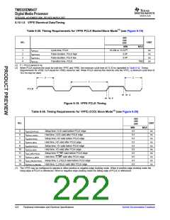
Table 6-35. Timing Requirements for VPFE PCLK Master/Slave Mode(1) (see Figure 6-19)
-400
-500
-600
NO.
UNIT
MIN
10.204 or 13.33(2)
0.4P
MAX
1
2
3
4
tc(PCLK)
tw(PCLKH)
tw(PCLKL)
tt(PCLK)
Cycle time, PCLK
ns
ns
ns
ns
Pulse duration, PCLK high
Pulse duration, PCLK low
Transition time, PCLK
0.4P
TBD
(1) P = PCLK period in ns.
(2) When PCLK sources the clock for both the VPFE and VPBE, the minimum cycle time of 13.33 ns (specified in Table 6-42, Timing
Requirements for VPBE CLK Inputs for VPBE) must be met. When PCLK sources the clock for only the VPFE, a minimum cycle time of
10.2 ns may be used.
2
3
1
PCLK
4
4
Figure 6-19. VPFE PCLK Timing
Table 6-36. Timing Requirements for VPFE (CCD) Slave Mode(1) (see Figure 6-20)
-400
-500
-600
NO.
UNIT
MIN
MAX
5
6
tsu(CCDV-PCLK)
th(PCLK-CCDV)
tsu(HDV-PCLK)
th(PCLK-HDV)
Setup time, CCD valid before PCLK edge
Hold time, CCD valid after PCLK edge
Setup time, HD valid before PCLK edge
Hold time, HD valid after PCLK edge
Setup time, VD valid before PCLK edge
Hold time, VD valid after PCLK edge
Setup time, C_WE valid before PCLK edge
Hold time, C_WE valid after PCLK edge
4.5
0.5
4.5
0.5
4.5
0.5
4.5
0.5
4.5
0.5
ns
ns
ns
ns
ns
ns
ns
ns
ns
ns
7
8
9
tsu(VDV-PCLK)
th(PCLK-VDV)
tsu(C_WEV-PCLK)
th(PCLK-C_WEV)
10
11
12
13
14
tsu(C_FIELDV-PCLK) Setup time, C_FIELD valid before PCLK edge
th(PCLK-C_FIELDV) Hold time, C_FIELD valid after PCLK edge
(1) The VPFE may be configured to operate in either positive or negative edge clocking mode. When in positive edge clocking mode the
rising edge of PCLK is referenced. When in negative edge clocking mode the falling edge of PCLK is referenced.
222
Peripheral Information and Electrical Specifications
Submit Documentation Feedback

 TI [ TEXAS INSTRUMENTS ]