TMS320DM6437
Digital Media Processor
www.ti.com
SPRS345B–NOVEMBER 2006–REVISED MARCH 2007
6.10.1.5 Histogram
The histogram module accepts raw image/video data and bins the pixels on a value (and color separate)
basis. The value of the pixel itself is not stored, but each bin contains the number of pixels that are within
the appropriate set range. The source of the raw data for the histogram is typically a CCD/CMOS sensor
(via the CCDC module) or optionally from DDR2. The following features are supported by the histogram
module.
•
•
•
Up to four regions/areas.
Separate horizontal/vertical start and end position for each region.
Pixels from overlapping regions are accumulated into the highest priority region. The priority is: region0
> region1 > region2 > region3.
•
•
•
•
•
•
Interface to conventional Bayer pattern. Each region can accumulate either 3 or 4 colors.
32, 64, 128, or 256 bins per color per region.
32, 64, or 128 bins per color for 2 regions.
32 or 64 bins per color for 3 or 4 regions.
Automatic clear of histogram RAM after an ARM read.
Saturation of the pixel count if the count exceeds the maximum value (each memory location is 20-bit
wide).
•
•
Downshift ranging from 0 to 7 bits (maximum bin range 128).
The last bin (highest range of values) will accumulate any value that is higher than the lower bound.
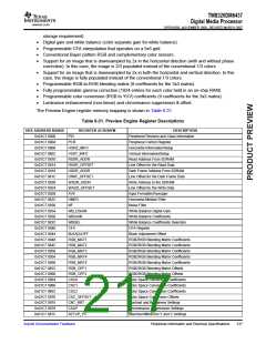
The Histogram register memory mapping is shown in Table 6-34.
Table 6-34. Histogram Register Descriptions
HEX ADDRESS RANGE
REGISTER ACRONYM
DESCRIPTION
0x01C7 1000
0x01C7 1004
0x01C7 1008
0x01C7 100C
0x01C7 1010
0x01C7 1014
0x01C7 1018
0x01C7 101C
0x01C7 1020
0x01C7 1024
0x01C7 1028
0x01C7 102C
0x01C7 1030
0x01C7 1034
0x01C7 1038
0x01C7 103C
0x01C7 1040
PID
Peripheral Revision and Class Information Register
Peripheral Control Register
PCR
HIST_CNT
WB_GAIN
R0_HORZ
R0_VERT
R1_HORZ
R1_VERT
R2_HORZ
R2_VERT
R3_HORZ
R3_VERT
HIST_ADDR
HIST_DATA
RADD
Histogram Control Bits Register
White/Channel Balance Settings Register
Region 0 Horizontal Information Register
Region 0 Vertical Information Register
Region 1 Horizontal Information Register
Region 1 Vertical Information Register
Region 2 Horizontal Information Register
Region 2 Vertical Information Register
Region 3 Horizontal Information Register
Region 3 Vertical Information Register
Histogram Address for Data to be Read Register
Histogram Data That is Read From the Memory Register
Read Address From DDR2 Memory Register
Read Address Offset for Each Line in the DDR2 Memory Register
RADD_OFF
H_V_INFO
Horizontal/Vertical Information Register (Horizontal/Vertical Number of
Pixels When Data is Read From DDR2 Memory Information Register)
Submit Documentation Feedback
Peripheral Information and Electrical Specifications
221

 TI [ TEXAS INSTRUMENTS ]