TMS320DM6437
Digital Media Processor
www.ti.com
SPRS345B–NOVEMBER 2006–REVISED MARCH 2007
6.10.2 Video Processing Back-End (VPBE)
The Video Processing Back-End (VPBE) consists of the On-Screen Display (OSD) module, the Video
Encoder (VENC) including the Digital LCD (DLCD) and Analog (i.e., DAC) interfaces. The video encoder
generates analog video output. The DLCD controller generates digital RGB/YCbCr data output and timing
signals.
Note: If the DAC is not used, for proper device operation connect the DAC pins as described in
Table 2-21, DAC [Part of VPBE] Terminal Functions.
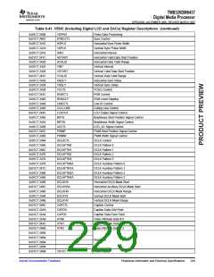
The VPBE register memory mapping is shown in Table 6-39.
Table 6-39. VPBE Register Descriptions
Address
Register
PID
Description
Peripheral Revision and Class Information Register
Peripheral Control Register
0x01C7 2780
0x01C7 2784
PCR
To ensure NTSC and PAL compliant output video, the stability of the input clock source is very important.
TI recommends a 27-MHz, 50-ppm crystal. Ceramic oscillators are not recommended. The NTSC/PAL
color sub-carrier frequency is derived from the 27-MHz clock; therefore, if the 27-MHz clock drifts, then the
color sub-carrier frequency will drift as well. Assuming no 27-MHz frequency drift, the color sub-carrier
frequency is generated as follows:
æ
ç
è
ö
÷
ø
35
f
= 27 MHz
= 3.5795454545 MHz
sc-ntsc
264
æ
ö
167
f
= 27 MHz
= 4.4332628318 MHz
ç
÷
sc- pal
1017
è
ø
To ensure the color sub-carrier frequency will not drift out of specification, the user must follow the crystal
requirements discussed in Section 6.6.1, Clock Input Option 1—Crystal.
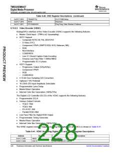
6.10.2.1 On-Screen Display (OSD)
The major function of the OSD module is to gather and blend video data and display/bitmap data before
feeding it to the Video Encoder (VENC) in YCbCr format. The video and display data is read from an
external memory, typically DDR2. The OSD is programmed via control and parameter registers. The
following are the primary features that are supported by the OSD.
•
Simultaneous display of two video windows and two OSD windows (VIDWIN0/VIDWIN1 and
OSDWIN0/OSDWIN1).
–
–
–
–
–
–
–
–
–
Separate enable for each window
Programmable width, height, and base starting coordinates for each window
External memory address and offset registers for each window
Support for x2 and x4 zoom in both the horizontal and vertical direction
OSDWIN1 can be used as an attribute window for OSDWIN0
Attribute window blinking intervals
Field/frame mode for the windows (interlaced/progressive)
Eight step blending process between the OSD and video windows
Transparency support for the OSD and video data (when a bitmap pixel is zero, there will be no
blending for that corresponding video pixel)
–
–
Resize from VGA to NTSC/PAL (640x480 to 720x576) for both the OSD and video windows
Reads in YCbCr data in 4:2:2 format from external memory, with the capability for swapping the
order of the CbCr component in the 32-bit word (this is relevant to the two video windows)
–
Support for a ping-pong buffer scheme that can be used for VIDWIN0 (allows for video data to be
accessed from two different locations in DDR2)
Submit Documentation Feedback
Peripheral Information and Electrical Specifications
225

 TI [ TEXAS INSTRUMENTS ]