TMS320DM6437
Digital Media Processor
www.ti.com
SPRS345B–NOVEMBER 2006–REVISED MARCH 2007
Default Power Down Pins
As discussed in Section 3.2, Power Considerations, the VDD3P3V_PWDN register controls power to the
3.3-V pins. The VDD3P3V_PWDN register defaults to powering down some 3.3-V pins to save power. For
more details on the VDD3P3V_PWDN register and which 3.3-V pins default to powerup or powerdown,
Section 3.2, Power Considerations. The pins that default to powerdown, are both reset to powerdown and
high-impedance. They remain in that state until configured otherwise by VDD3P3_PWDN and
PINMUX0/PINMUX1 programming.
•
Default Power Down Pin Group: GP[4]/PWM1, ACLKR0/CLKX0/GP[99], AFSR0/DR0/GP[100],
AHCLKR0/CLKR0/GP[101], AXR0[3]/FSR0/GP[102], AXR0[2]/FSX0/GP[103], AXR0[1]/DX0/GP[104],
AXR0/FSR1/GP[105], ACLKX0/CLKX1/GP[106], AFSX0/DX1/GP[107], AHCLKX0/CLKR1/GP[108],
AMUTEIN0/FSX1/GP[109], AMUTE0/DR1/GP[110], HECC_TX/TOUT1L/UTXD1/GP[55],
HECC_RX/TINP1L/URXD1/GP[56], CLKS0/TOUT0L/GP[97], CLKS1/TINP0L/GP[98], URXD0/GP[85],
UTXD0/GP[86], UCTS0/GP[87], and URTS0/PWM0/GP[88].
All Other Pins
During RESETOUT assertion (low), all other pins are controlled by the default peripheral. The default
peripheral is determined by the default settings of the PINMUX0 or PINMUX1 registers.
Some of the PINMUX0/PINMUX1 settings are determined by configuration pins latched at reset. To
determine the reset behavior of these pins, see Section 3.7, Multiplexed Pin Configurations and read the
rest of the this subsection to understand how that default peripheral controls the pin.
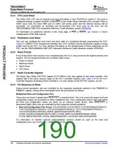
The reset behaviors for all these other pins are categorized as follows (also see Figure 6-7 and Figure 6-8
in Section 6.5.9, Reset Electrical Data/Timing):
•
•
•
Z+/Low Group (Z Longer-to-Low Group): These pins are 3-stated when device-level global reset
source (e.g., POR, RESET, or Max Reset) is asserted. These pins remain 3-stated throughout
RESETOUT assertion. When RESETOUT is deasserted, these pins drive a logic low.
Z+/High Group (Z Longer-to-High Group): These pins are 3-stated when device-level global reset
source (e.g., POR, RESET, or Max Reset) is asserted. These pins remain 3-stated throughout
RESETOUT assertion. When RESETOUT is deasserted, these pins drive a logic high.
Z+/Invalid Group (Z Longer-to-Invalid Group): These pins are 3-stated when device-level global
reset source (e.g., POR, RESET, or Max Reset) is asserted. These pins remain 3-stated throughout
RESETOUT assertion. When RESETOUT is deasserted, these pins drive an invalid value until
configured otherwise by their respective peripheral (after the peripheral is enabled by the PSC).
•
Z Group: These pins are 3-stated by default, and these pins remain 3-stated throughout RESETOUT
assertion. When RESETOUT is deasserted, these pins remain 3-stated until configured otherwise by
their respective peripheral (after the peripheral is enabled by the PSC).
•
•
•
Low Group: These pins are low by default, and remain low until configured otherwise by their
respective peripheral (after the peripheral is enabled by the PSC).
High Group: These pins are high by default, and remain high until configured otherwise by their
respective peripheral (after the peripheral is enabled by the PSC).
Z/Low Group (Z-to-Low Group): These pins are 3-stated when device-level global reset source (e.g.,
POR, RESET, or Max Reset) is asserted. When the reset source is deasserted, these pins drive a
logic low.
•
•
Z/High Group (Z-to-High Group): These pins are 3-stated when device-level global reset source
(e.g., POR, RESET, or Max Reset) is asserted. When reset source is deasserted, these pins drive a
logic high.
Clock Group: These clock pins are toggling by default. They paused momentarily before RESETOUT
is deasserted (high). The only pin in the Clock Group is CLKOUT0.
This is a list of possible default peripherals and how they control the pins during reset:
•
GPIO: All GPIO pins behave according to Z Group.
Note: The following EMIFA list only includes pins that can default to function as EMIFA signals.
Submit Documentation Feedback
Peripheral Information and Electrical Specifications
191

 TI [ TEXAS INSTRUMENTS ]