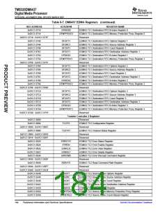
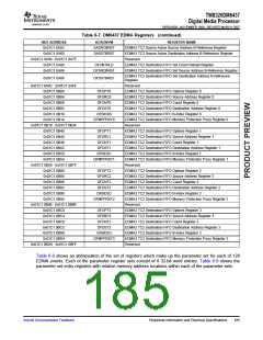
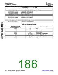
TMS320DM6437
Digital Media Processor
www.ti.com
SPRS345B–NOVEMBER 2006–REVISED MARCH 2007
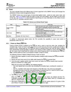
At this point:
–
The I/O pins are controlled by the default peripherals (default peripherals are determined by
PINMUX0 and PINMUX1 registers).
–
The clock and reset of each peripheral is determined by the default settings of the Power and Sleep
Controller (PSC).
–
–
The PLL Controllers are operating in PLL Bypass Mode.
The C64x+ begins executing from DSPBOOTADDR (determined by bootmode selection).
After the reset sequence, the boot sequence begins. For more details on the boot sequence, see the
Using the TMS320DM643x Bootloader Application Report (literature number SPRAAG0).
After the boot sequence, follow the software initialization sequence described in Section 3.8, Device
Initialization Sequence After Reset.
6.5.1.1 Usage of POR versus RESET Pins
POR and RESET are independent resets.
If the device needs to go through a power-up cycle, POR (not RESET) must be used to fully reset the
device.
In functional end-system, emulation/debugger logic is typically not needed; therefore, the recommendation
for functional end-system is to use the POR pin for full device reset. If RESET pin is not needed, it can be
pulled inactive (high) via an external pullup resistor.
In a debug system, it is typically desirable to allow the reset of the device without crashing an emulation
session. In this case, the user can use the POR pin to achieve full device reset and use the RESET pin to
achieve a debug reset—which resets the entire device except emulation logic.
6.5.1.2 Latching Boot and Configuration Pins
Internal to the chip, the two device reset pins RESET and POR are logically AND’d together only for the
purpose of latching device boot and configuration pins. The values on all device and boot configuration
pins are latched into the BOOTCFG register when the logical AND of RESET and POR transitions from
low-to-high.
6.5.2 Warm Reset (RESET Pin)
A Warm Reset is activated by driving the RESET pin active low. This resets everything in the device
except the emulation logic. An emulator session will stay alive during warm reset.
For more information on POR vs. RESET usage, see Section 6.5.1.1, Usage of POR versus RESET Pins
and Section 6.5.1.2, Latching Boot and Configuration Pins.
The following sequence must be followed during a Warm Reset:
1. Power supplies and input clock source should already be stable.
2. The RESET pin must be asserted (low) for a minimum of 12 MXI cycles.
Within the low period of the RESET pin, the following happens:
–
–
–
The reset signals flow to the entire chip resetting all the modules on chip, except the emulation
logic.
The PLL Controllers are reset thereby, switching back to PLL Bypass Mode and resetting all their
registers to default values. Both PLL1 and PLL2 are placed in reset and lose lock.
The RESETOUT pin becomes asserted (low), indicating the device is in reset.
3. The POR pin may now be deasserted (driven high).
When the POR pin is deasserted (high), the configuration pin values are latched and the PLL
Controllers changed their system clocks to their default divide-down values. Both PLL Controllers are
still in PLL Bypass Mode. Other device initialization also begins.
4. After device initialization is complete, the PLL Controllers pause the system clocks for 10 cycles. At the
end of these 10 cycles, the RESETOUT pin is deasserted (driven high).
188
Peripheral Information and Electrical Specifications
Submit Documentation Feedback

 TI [ TEXAS INSTRUMENTS ]