TMS320DM6437
Digital Media Processor
www.ti.com
SPRS345B–NOVEMBER 2006–REVISED MARCH 2007
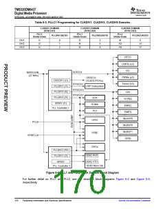
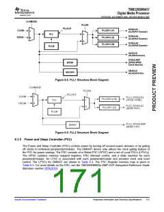
CLKMODE
PLLEN
PLLOUT
SYSCLK1
PLLDIV1 (/1)
CLKIN
OSCIN
1
0
(CLKDIV1 Domain)
PLL
1
0
SYSCLK2
PLLDIV2 (/3)
(CLKDIV3 Domain)
SYSCLK3
PLLDIV3 (/6)
(CLKDIV6 Domain)
PLLM
AUXCLK
(CLKIN Domain)
SYSCLKBP
(VPSS-VPBE
Clock Source)
BPDIV
OBSCLK
(CLKOUT0 Pin)
OSCDIV1
Figure 6-5. PLL1 Structure Block Diagram
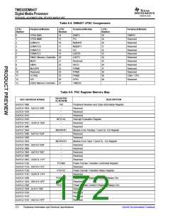
CLKMODE
PLLEN
PLLOUT
CLKIN
OSCIN
1
0
PLL2_SYSCLK2
(VPSS−VPBE)
PLLDIV2 (/10)
PLL
1
0
PLL2_SYSCLK1
(DDR2 PHY)
PLLDIV1 (/2)
PLLM
PLL2_SYSCLKBP
(DDR2 VTP)
BPDIV
Figure 6-6. PLL2 Structure Block Diagram
6.3.5 Power and Sleep Controller (PSC)
The Power and Sleep Controller (PSC) controls power by turning off unused power domains or by gating
off clocks to individual peripherals/modules. The DM6437 device only utilizes the clock gating feature of
the PSC for power savings. The PSC consists of a Global PSC (GPSC) and a set of Local PSCs (LPSCs).
The GPSC contains memory mapped registers, PSC interrupt control, and a state machine for each
peripheral/module. An LPSC is associated with each peripheral/module and provides clock and reset
control. The LPSCs for DM6437 are shown in Table 6-4. The PSC Register memory map is given in
Table 6-5. For more details on the PSC, see the TMS320DM643x DMP DSP Subsystem Reference Guide
(literature number SPRU978).
Submit Documentation Feedback
Peripheral Information and Electrical Specifications
171

 TI [ TEXAS INSTRUMENTS ]