TMS320DM6437
Digital Media Processor
www.ti.com
SPRS345B–NOVEMBER 2006–REVISED MARCH 2007
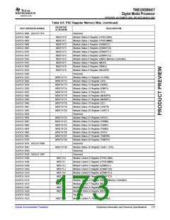
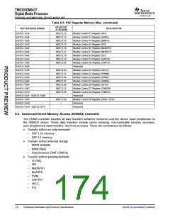
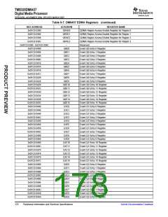
Table 6-5. PSC Register Memory Map (continued)
REGISTER
ACRONYM
HEX ADDRESS RANGE
0x01C4 1A30
DESCRIPTION
MDCTL12
MDCTL13
MDCTL14
MDCTL15
MDCTL16
MDCTL17
MDCTL18
MDCTL19
MDCTL20
–
Module Control 12 Register (HPI)
0x01C4 1A34
Module Control 13 Register (DDR2)
Module Control 14 Register (EMIFA)
Module Control 15 Register (PCI)
Module Control 16 Register (McBSP0)
Module Control 17 Register (McBSP1)
Module Control 18 Register (I2C)
Module Control 19 Register (UART0)
Module Control 20 Register (UART1)
Reserved
0x01C4 1A38
0x01C4 1A3C
0x01C4 1A40
0x01C4 1A44
0x01C4 1A48
0x01C4 1A4C
0x01C4 1A50
0x01C4 1A54
0x01C4 1A58
MDCTL22
MDCTL23
MDCTL24
MDCTL25
MDCTL26
MDCTL27
MDCTL28
–
Module Control 22 Register (HECC)
Module Control 23 Register (PWM0)
Module Control 24 Register (PWM1)
Module Control 25 Register (PWM2)
Module Control 26 Register (GPIO)
Module Control 27 Register (TIMER0)
Module Control 28 Register (TIMER1)
Reserved
0x01C4 1A5C
0x01C4 1A60
0x01C4 1A64
0x01C4 1A68
0x01C4 1A6C
0x01C4 1A70
0x01C4 1A74 - 0x01C4 1A9B
0x01C4 1A9C
0x01C4 1AA0
MDCTL39
–
Module Control 39 Register (C64x+ CPU)
Reserved
0x01C4 1AA4 - 0x01C4 1FFF
–
Reserved
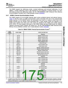
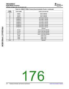
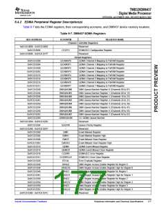
6.4 Enhanced Direct Memory Access (EDMA3) Controller
The EDMA controller handles all data transfers between memories and the device slave peripherals on
the DM6437 device. These data transfers include cache servicing, non-cacheable memory accesses,
user-programmed data transfers, and host accesses. These are summarized as follows:
•
Transfer to/from on-chip memories
–
–
DSP L1D memory
DSP L2 memory
•
Transfer to/from external storage
–
–
–
DDR2 SDRAM
NAND flash
Asynchronous EMIF (EMIFA)
•
Transfer to/from peripherals/hosts
–
–
–
–
–
–
–
–
VLYNQ
HPI
McBSP0/1
McASP0
PWM
UART0/1
HECC
PCI
174
Peripheral Information and Electrical Specifications
Submit Documentation Feedback

 TI [ TEXAS INSTRUMENTS ]