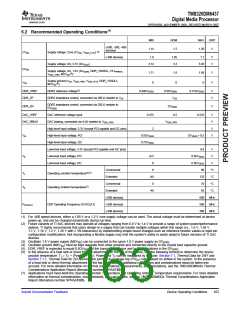
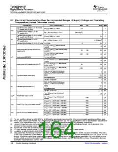
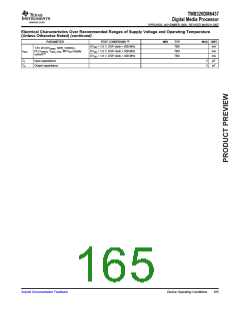
TMS320DM6437
Digital Media Processor
www.ti.com
SPRS345B–NOVEMBER 2006–REVISED MARCH 2007
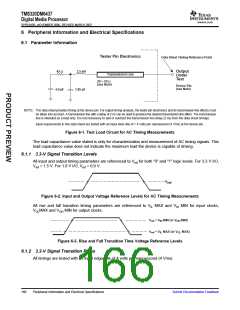
6.1.3 Timing Parameters and Board Routing Analysis
The timing parameter values specified in this data sheet do not include delays by board routings. As a
good board design practice, such delays must always be taken into account. Timing values may be
adjusted by increasing/decreasing such delays. TI recommends utilizing the available I/O buffer
information specification (IBIS) models to analyze the timing characteristics correctly. To properly use IBIS
models to attain accurate timing analysis for a given system, see the Using IBIS Models for Timing
Analysis application report (literature number SPRA839). If needed, external logic hardware such as
buffers may be used to compensate any timing differences.
For the DDR2 memory controller interface, it is not necessary to use the IBIS models to analyze timing
characteristics. TI provides a PCB routing rules solution that describes the routing rules to ensure the
DDR2 memory controller interface timings are met. See the Implementing DDR2 PCB Layout on the
TMS320DM643x DMP Application Report (literature number TBD).
6.2 Recommended Clock and Control Signal Transition Behavior
All clocks and control signals must transition between VIH and VIL (or between VIL and VIH) in a monotonic
manner.
6.3 Power Supplies
For more information regarding TI's power management products and suggested devices to power TI
DSPs, visit www.ti.com/dsppower.
6.3.1 Power-Supply Sequencing
The DM6437 includes one core supply (CVDD), and two I/O supplies—DVDD33 and DVDDR2. To ensure
proper device operation, a specific power-up sequence must be followed. Some TI power-supply devices
include features that facilitate power sequencing—for example, Auto-Track and Slow-Start/Enable
features. For more information on TI power supplies and their features, visit www.ti.com/dsppower.
Here is a summary of the power sequencing requirements:
•
The power ramp order must be DVDD33 before DVDDR2, and DVDDR2 before CVDD—meaning during
power up, the voltage at the DVDDR2 rail should never exceed the voltage at the DVDD33 rail. Similarly,
the voltage at the CVDD rail should never exceed the voltage at the DVDDR2 rail.
•
From the time that power ramp begins, all power supplies (DVDD33, DVDDR2, CVDD) must be stable
within 200 ms. The term "stable" means reaching the recommended operating condition (see
Section 5.2, Recommended Operating Conditions table).
6.3.2 Power-Supply Design Considerations
Core and I/O supply voltage regulators should be located close to the DSP to minimize inductance and
resistance in the power delivery path. Additionally, when designing for high-performance applications
utilizing the DM6437 device, the PC board should include separate power planes for core, I/O, and
ground; all bypassed with high-quality low-ESL/ESR capacitors.
6.3.3 Power-Supply Decoupling
In order to properly decouple the supply planes from system noise, place as many capacitors (caps) as
possible close to the DSP. These caps need to be close to the DSP, no more than 1.25 cm maximum
distance to be effective. Physically smaller caps are better, such as 0402, but need to be evaluated from a
yield/manufacturing point-of-view. Parasitic inductance limits the effectiveness of the decoupling
capacitors, therefore physically smaller capacitors should be used while maintaining the largest available
capacitance value.
Larger caps for each supply can be placed further away for bulk decoupling. Large bulk caps (on the order
of 100 µF) should be furthest away, but still as close as possible. Large caps for each supply should be
placed outside of the BGA footprint.
Submit Documentation Feedback
Peripheral Information and Electrical Specifications
167

 TI [ TEXAS INSTRUMENTS ]