TMS320C6678
Multicore Fixed and Floating-Point Digital Signal Processor
SPRS691D—April 2013
www.ti.com
3.3.4 Kicker Mechanism (KICK0 and KICK1) Register
The Bootcfg module contains a kicker mechanism to prevent any spurious writes from changing any of the Bootcfg
MMR values. When the kicker is locked (which it is initially after power on reset) none of the Bootcfg MMRs are
writable (they are only readable). This mechanism requires two MMR writes to the KICK0 and KICK1 registers with
exact data values before the kicker lock mechanism is un-locked. See Table 3-2 ‘‘Device State Control Registers’’ on
page 75 for the address location. Once released then all the Bootcfg MMRs having “write” permissions are writable
(the read only MMRs are still read only). The first KICK0 data is 0x83e70b13. The second KICK1 data is 0x95a4f1e0.
Writing any other data value to either of these kick MMRs will lock the kicker mechanism and block any writes to
Bootcfg MMRs.
The kicker mechanism is unlocked by the ROM code. Do not write any other different values afterward to these
registers because that will lock the kicker mechanism and block any writes to Bootcfg registers.
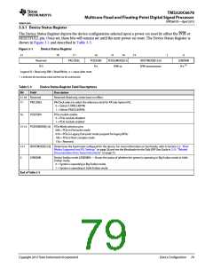
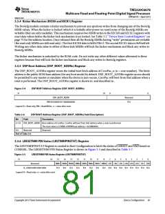
3.3.5 DSP Boot Address (DSP_BOOT_ADDRn) Register
The DSP_BOOT_ADDRn register stores the initial boot fetch address of CorePac_n (n = core number). The fetch
address is the public ROM base address (for any boot mode) by default. DSP_BOOT_ADDRn register access should
be permitted to any master or emulator when the device is non-secure. CorePac will boot from that address when a
reset is performed. The DSP_BOOT_ADDRn register is shown in and described in .
Figure 3-4
DSP BOOT Address Register (DSP_BOOT_ADDRn)
31
10
9
0
DSP_BOOT_ADDR
Reserved
R-0
RW-0010000010110000000000
Legend: R = Read only; RW = Read/Write; -n = value after reset
Table 3-6
DSP BOOT Address Register (DSP_BOOT_ADDRn) Field Descriptions
Bit
Field
Description
31-10 DSP_BOOT_ADDR Boot address of CorePac. CorePac will boot from that address when a reset is performed.
The reset value is 22 MSBs of ROM base address = 0x20B00000.
9-0
Reserved
Reserved
End of Table 3-6
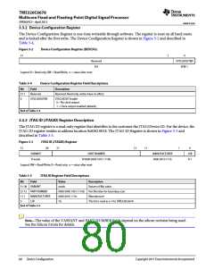
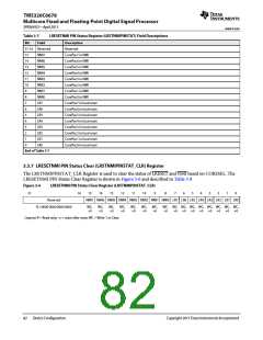
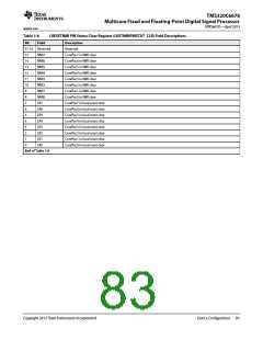
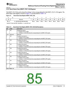
3.3.6 LRESETNMI PIN Status (LRSTNMIPINSTAT) Register
The LRSTNMIPINSTAT Register is created in Boot Configuration to latch the status of LRESET and NMI based on
CORESEL. The LRESETNMI PIN Status Register is shown in Figure 3-5 and described in Table 3-7.
Figure 3-5
LRESETNMI PIN Status Register (LRSTNMIPINSTAT)
31
16
15
14
13
12
11
10
9
8
7
6
5
4
3
2
1
0
Reserved
R, +0000 0000 0000 0000
Legend: R = Read only; -n = value after reset
NMI7 NMI6 NMI5 NMI4 NMI3 NMI2 NMI1 NMI0 LR7 LR6 LR5 LR4 LR3 LR2 LR1 LR0
R-0
R-0
R-0
R-0
R-0
R-0
R-0
R-0 R-0 R-0 R-0 R-0 R-0 R-0 R-0 R-0
Copyright 2013 Texas Instruments Incorporated
Device Configuration 81

 TI [ TEXAS INSTRUMENTS ]