TMS320C6672
Multicore Fixed and Floating-Point Digital Signal Processor
SPRS708C—February 2012
www.ti.com
1 Some of the PKTDMA-based peripherals require multiple master IDs. QMS_PKTDMA is assigned with 88,89,90,91, but only 88-89 are actually used. For Network coprocessor
packet DMA port, 56,57,58,59 are assigned while only 1 (56) is actually used. There are two master ID values are assigned for the QM_second master port, one master ID
for external linking RAM and the other one for the PDSP/MCDM accesses.
2 The master ID for MSMC is for the transactions initiated by MSMC internally and sent to the DDR.
3 All CP_traces are set to the same master ID and bit 7 of the master ID needs to be 1.
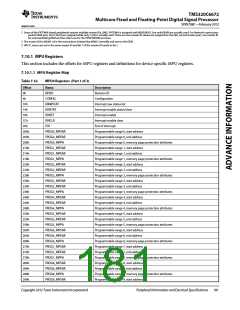
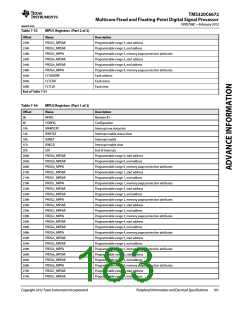
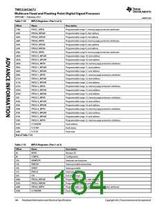
7.10.1 MPU Registers
This section includes the offsets for MPU registers and definitions for device specific MPU registers.
7.10.1.1 MPU Register Map
Table 7-52
MPU0 Registers (Part 1 of 2)
Offset
0h
Name
Description
REVID
Revision ID
4h
CONFIG
Configuration
10h
IRAWSTAT
Interrupt raw status/set
14h
IENSTAT
Interrupt enable status/clear
18h
IENSET
Interrupt enable
1Ch
IENCLR
Interrupt enable clear
20h
EOI
End of interrupt
200h
204h
208h
210h
214h
218h
220h
224h
228h
230h
234h
238h
240h
244h
248h
250h
254h
258h
260h
264h
268h
270h
274h
278h
280h
284h
288h
290h
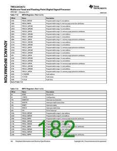
PROG0_MPSAR
PROG0_MPEAR
PROG0_MPPA
PROG1_MPSAR
PROG1_MPEAR
PROG1_MPPA
PROG2_MPSAR
PROG2_MPEAR
PROG2_MPPA
PROG3_MPSAR
PROG3_MPEAR
PROG3_MPPA
PROG4_MPSAR
PROG4_MPEAR
PROG4_MPPA
PROG5_MPSAR
PROG5_MPEAR
PROG5_MPPA
PROG6_MPSAR
PROG6_MPEAR
PROG6_MPPA
PROG7_MPSAR
PROG7_MPEAR
PROG7_MPPA
PROG8_MPSAR
PROG8_MPEAR
PROG8_MPPA
PROG9_MPSAR
Programmable range 0, start address
Programmable range 0, end address
Programmable range 0, memory page protection attributes
Programmable range 1, start address
Programmable range 1, end address
Programmable range 1, memory page protection attributes
Programmable range 2, start address
Programmable range 2, end address
Programmable range 2, memory page protection attributes
Programmable range 3, start address
Programmable range 3, end address
Programmable range 3, memory page protection attributes
Programmable range 4, start address
Programmable range 4, end address
Programmable range 4, memory page protection attributes
Programmable range 5, start address
Programmable range 5, end address
Programmable range 5, memory page protection attributes
Programmable range 6, start address
Programmable range 6, end address
Programmable range 6, memory page protection attributes
Programmable range 7, start address
Programmable range 7, end address
Programmable range 7, memory page protection attributes
Programmable range 8, start address
Programmable range 8, end address
Programmable range 8, memory page protection attributes
Programmable range 9, start address
Copyright 2012 Texas Instruments Incorporated
Peripheral Information and Electrical Specifications 181

 TI [ TEXAS INSTRUMENTS ]