TMS320C6672
Multicore Fixed and Floating-Point Digital Signal Processor
SPRS708C—February 2012
www.ti.com
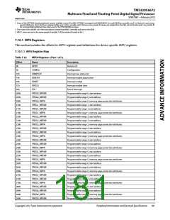
Table 7-55
MPU3 Registers (Part 2 of 2)
Offset
304h
Name
Description
Fault status
Fault clear
FLTSTAT
FLTCLR
308h
End of Table 7-55
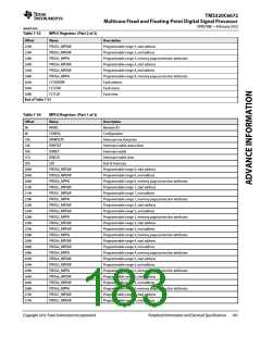
7.10.1.2 Device-Specific MPU Registers
7.10.1.2.1 Configuration Register (CONFIG)
The configuration register (CONFIG) contains the configuration value of the MPU.
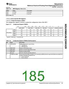
Figure 7-31
Configuration Register (CONFIG)
31
24
23
20
19
16
15
12
11
1
0
ADDR_WIDTH
NUM_FIXED
NUM_PROG
R-16
NUM_AIDS
R-16
Reserved
R-0
ASSUME_ALLOWED
MPU0
MPU1
MPU2
MPU3
R-0
R-0
R-0
R-0
R-0
R-0
R-0
R-0
R-1
R-1
R-1
R-1
R-5
R-16
R-0
Reset Values
R-16
R-16
R-0
R-1
R-16
R-0
Legend: R = Read only; -n = value after reset
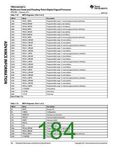
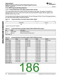
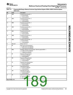
Table 7-56
Configuration Register (CONFIG) Field Descriptions
Bit
Field Description
31 – 24 ADDR_WIDTH
Address alignment for range checking
0 = 1KB alignment
6 = 64KB alignment
23 – 20 NUM_FIXED
19 – 16 NUM_PROG
15 – 12 NUM_AIDS
Number of fixed address ranges
Number of programmable address ranges
Number of supported AIDs
11 – 1
0
Reserved
Reserved. These bits will always reads as 0.
ASSUME_ALLOWED
Assume allowed bit. When an address is not covered by any MPU protection range, this bit determines whether the
transfer is assumed to be allowed or not.
0 = Assume disallowed
1 = Assume allowed
Copyright 2012 Texas Instruments Incorporated
Peripheral Information and Electrical Specifications 185

 TI [ TEXAS INSTRUMENTS ]