TMS320C6672
Multicore Fixed and Floating-Point Digital Signal Processor
SPRS708C—February 2012
www.ti.com
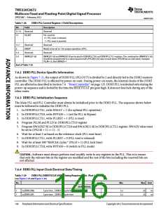
Table 7-28
DDR3 PLL Control Register 1 Field Descriptions
Description
Bit
Field
Reserved
31-14
13
Reserved
PLLRST
PLL reset bit.
0 = PLL reset is released.
1 = PLL reset is asserted.
12-7
6
Reserved
ENSAT
Reserved
Needs to be set to 1 for proper operation of PLL
Reserved
5-4
3-0
Reserved
BWADJ[11:8]
BWADJ[11:8] and BWADJ[7:0] are located in DDR3PLLCTL0 and DDR3PLLCTL1 registers. The combination (BWADJ[11:0])
should be programmed to a value equal to half of PLLM[12:0] value (round down if PLLM has an odd value). Example:
PLLM=15, then BWADJ=7
End of Table 7-28
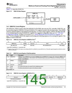
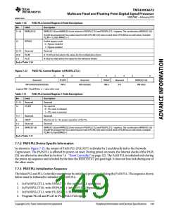
7.6.2 DDR3 PLL Device-Specific Information
As shown in Figure 7-21, the output of DDR3 PLL (PLLOUT) is divided by 2 and directly fed to the DDR3 memory
controller. The DDR3 PLL is affected by power-on reset. During power-on resets, the internal clocks of the DDR3
PLL are affected as described in Section 7.4 ‘‘Reset Controller’’ on page 125. DDR3 PLL is unlocked only during the
power-up sequence and is locked by the time the RESETSTAT pin goes high. It does not lose lock during any of the
other resets.
7.6.3 DDR3 PLL Initialization Sequence
The Main PLL and PLL Controller must always be initialized prior to the DDR3 PLL. The sequence shown below
must be followed to initialize the DDR3 PLL.
1. In DDR3PLLCTL1, write ENSAT = 1 (for optimal PLL operation)
2. In DDR3PLLCTL0, write BYPASS = 1 (set the PLL in Bypass)
3. In DDR3PLLCTL1, write PLLRST = 1 (PLL is reset)
4. Program PLLM and PLLD in DDR3PLLCTL0 register
5. Program BWADJ[7:0] in DDR3PLLCTL0 and BWADJ[11:8] in DDR3PLLCTL1 register. BWADJ value must
be set to ((PLLM + 1) >> 1) - 1)
6. Wait for at least 5 us based on the reference clock (PLL reset time)
7. In DDR3PLLCTL1, write PLLRST = 0 (PLL reset is released)
8. Wait for at least 500 *REFCLK cycles * (PLLD + 1) (PLL lock time)
9. In DDR3PLLCTL0, write BYPASS = 0 (switch to PLL mode)
CAUTION—Software must always perform read-modify-write to any registers in the PLL. This is to ensure
that only the relevant bits in the register are modified and the rest of the bits including the reserved bits are
not affected.
7.6.4 DDR3 PLL Input Clock Electrical Data/Timing
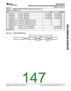
Table 7-29
DDR3 PLL DDRSYSCLK1(N|P) Timing Requirements (Part 1 of 2)
(see Figure 7-24 and Figure 7-20)
No.
Min
Max Unit
DDRCLK[P:N]
1
1
tc(DDRCLKN)
tc(DDRCLKP)
Cycle time _ DDRCLKN cycle time
Cycle time _ DDRCLKP cycle time
3.2
3.2
25
25
ns
ns
146
Peripheral Information and Electrical Specifications
Copyright 2012 Texas Instruments Incorporated

 TI [ TEXAS INSTRUMENTS ]