TMS320C6672
Multicore Fixed and Floating-Point Digital Signal Processor
SPRS708C—February 2012
www.ti.com
5. Program BWADJ[7:0] in PASSPLLCTL0 and BWADJ[11:8] in PASSPLLCTL1 register. BWADJ value must
be set to ((PLLM + 1) >> 1) - 1)
6. Wait for at least 5 us based on the reference clock (PLL reset time)
7. In PASSPLLCTL1, write PLLRST = 0 (PLL reset is released)
8. Wait for at least 500 * REFCLK cycles * (PLLD + 1) (PLL lock time)
9. In PASSPLLCTL0, write BYPASS = 0 (switch to PLL mode)
CAUTION—Software must always perform read-modify-write to any registers in the PLL. This is to ensure
that only the relevant bits in the register are modified and the rest of the bits including the reserved bits are
not affected.
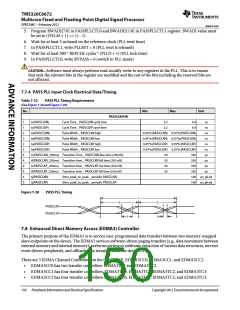
7.7.4 PASS PLL Input Clock Electrical Data/Timing
Table 7-32
PASS PLL Timing Requirements
(See Figure 7-28 and Figure 7-20)
No.
Min
Max
Unit
PASSCLK[P:N]
1
1
3
2
2
3
4
4
4
4
5
5
tc(PASSCLKN)
tc(PASSCLKP)
tw(PASSCLKN)
tw(PASSCLKN)
tw(PASSCLKP)
tw(PASSCLKP)
Cycle Time _ PASSCLKN cycle time
Cycle Time _ PASSCLKP cycle time
Pulse Width _ PASSCLKN high
Pulse Width _ PASSCLKN low
Pulse Width _ PASSCLKP high
Pulse Width _ PASSCLKP low
3.2
3.2
6.4
6.4
ns
ns
ns
ns
ns
ns
ps
ps
ps
ps
0.45*tc(PASSCLKN) 0.55*tc(PASSCLKN)
0.45*tc(PASSCLKN) 0.55*tc(PASSCLKN)
0.45*tc(PASSCLKP) 0.55*tc(PASSCLKP)
0.45*tc(PASSCLKP) 0.55*tc(PASSCLKP)
tr(PASSCLKN_250mv) Transition Time _ PASSCLKN Rise time (250mV)
tf(PASSCLKN_250mv) Transition time _ PASSCLKN fall time (250 mV)
tr(PASSCLKP_250mv) Transition time _ PASSCLKP rise time (250 mV)
tf(PASSCLKP_250mv) Transition time _ PASSCLKP fall time (250 mV)
50
50
50
50
350
350
350
350
tj(PASSCLKN)
tj(PASSCLKP)
Jitter, peak_to_peak _ periodic PASSCLKN
Jitter, peak_to_peak _ periodic PASSCLKP
100 ps, pk-pk
100 ps, pk-pk
Figure 7-28
PASS PLL Timing
1
2
3
5
PASSCLKN
PASSCLKP
4
7.8 Enhanced Direct Memory Access (EDMA3) Controller
The primary purpose of the EDMA3 is to service user-programmed data transfers between two memory-mapped
slave endpoints on the device. The EDMA3 services software-driven paging transfers (e.g., data movement between
external memory and internal memory), performs sorting or subframe extraction of various data structures, services
event driven peripherals, and offloads data transfers from the device CPU.
There are 3 EDMA Channel Controllers on the C6672 DSP, EDMA3CC0, EDMA3CC1, and EDMA3CC2.
•
•
•
EDMA3CC0 has two transfer controllers: EDMA3TC1 and EDMA3TC2.
EDMA3CC1 has four transfer controllers: EDMA3TC0, EDMA3TC1, EDMA3TC2, and EDMA3TC3.
EDMA3CC2 has four transfer controllers: EDMA3TC0, EDMA3TC1, EDMA3TC2, and EDMA3TC3.
150
Peripheral Information and Electrical Specifications
Copyright 2012 Texas Instruments Incorporated

 TI [ TEXAS INSTRUMENTS ]