TMS320C6672
Multicore Fixed and Floating-Point Digital Signal Processor
SPRS708C—February 2012
www.ti.com
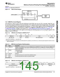
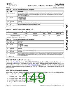
Figure 7-21 shows the DDR3 PLL.
Figure 7-21
DDR3 PLL Block Diagram
DDR3 PLL
PLLD xPLLM /2
0
DDRCLK(N|P)
PLLOUT
DDR3
PHY
1
BYPASS
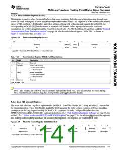
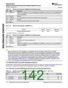
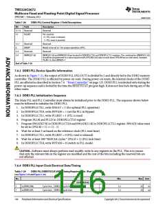
7.6.1 DDR3 PLL Control Register
The DDR3 PLL, which is used to drive the DDR PHY for the EMIF, does not use a PLL controller. DDR3 PLL can
be controlled using the DDR3PLLCTL0 and DDR3PLLCTL1 registers located in the Bootcfg module. These MMRs
(memory-mapped registers) exist inside the Bootcfg space. To write to these registers, software should go through
an un-locking sequence using KICK0/KICK1 registers. For suggested configurable values see 2.5.3 ‘‘PLL Boot
Configuration Settings’’ on page 34. See section 3.3.4 ‘‘Kicker Mechanism (KICK0 and KICK1) Register’’ on
page 77 for the address location of the registers and locking and unlocking sequences for accessing the registers. This
register is reset on POR only
.
Figure 7-22
DDR3 PLL Control Register 0 (DDR3PLLCTL0) (1)
31
24
23
22
Reserved
RW,+0001
19
18
6
5
0
BWADJ[7:0]
RW,+0000 1001
BYPASS
RW,+0
PLLM
PLLD
RW,+000000
RW,+0000000010011
Legend: RW = Read/Write; -n = value after reset
1 This register is Reset on POR only. The regreset, reset and bgreset from PLL are all tied to a common pll0_ctrl_rst_n The pwrdn, regpwrdn, bgpwrdn are all tied to common
pll0_ctrl_to_pll_pwrdn.
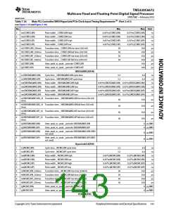
Table 7-27
DDR3 PLL Control Register 0 Field Descriptions
Description
Bit
Field
BWADJ[7:0]
31-24
BWADJ[11:8] and BWADJ[7:0] are located in DDR3PLLCTL0 and DDR3PLLCTL1 registers. The combination (BWADJ[11:0])
should be programmed to a value equal to half of PLLM[12:0] value (round down if PLLM has an odd value). Example:
PLLM=15, then BWADJ=7
23
BYPASS
Enable bypass mode
0 = Bypass disabled
1 = Bypass enabled
22-19
18-6
5-0
Reserved
PLLM
Reserved
A 13-bit bus that selects the values for the multiplication factor
A 6-bit bus that selects the values for the reference divider
PLLD
End of Table 7-27
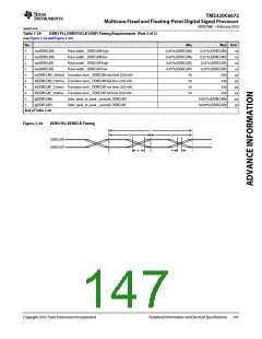
Figure 7-23
DDR3 PLL Control Register 1 (DDR3PLLCTL1)
31
14
13
12
7
6
5
4
3
0
Reserved
RW-000000000000000000
Legend: RW = Read/Write; -n = value after reset
PLLRST
RW-0
Reserved
ENSAT
RW-0
Reserved
R-0
BWADJ[11:8]
RW-0000
RW-000000
Copyright 2012 Texas Instruments Incorporated
Peripheral Information and Electrical Specifications 145

 TI [ TEXAS INSTRUMENTS ]