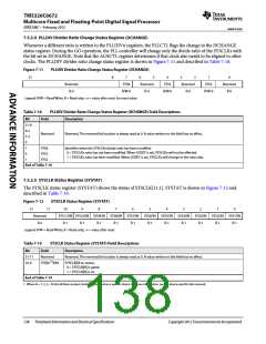
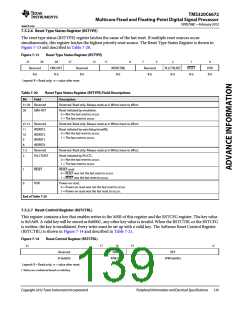
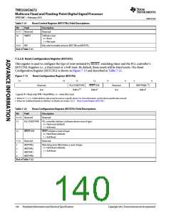
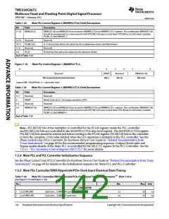
TMS320C6672
Multicore Fixed and Floating-Point Digital Signal Processor
SPRS708C—February 2012
www.ti.com
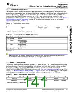
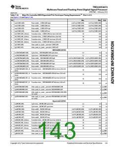
Table 7-24
Main PLL Control Register 0 (MAINPLLCTL0) Field Descriptions
Bit
Field Description
31-24
BWADJ[7:0]
BWADJ[11:8] and BWADJ[7:0] are located in MAINPLLCTL0 and MAINPLLCTL1 registers. The combination (BWADJ[11:0])
should be programmed to a value equal to half of PLLM[12:0] value (round down if PLLM has an odd value). Example:
PLLM=15, then BWADJ=7
23-19
18-12
11-6
5-0
Reserved
PLLM[12:6]
Reserved
PLLD
Reserved
A 13-bit bus that selects the values for the multiplication factor (see Note below)
Reserved
A 6-bit bus that selects the values for the reference divider
End of Table 7-24
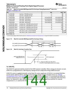
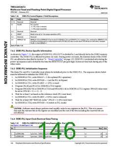
Figure 7-18
Main PLL Control Register 1 (MAINPLLCTL1)
31
7
6
5
4
3
0
Reserved
ENSAT
RW-0
Reserved
RW-00
BWADJ[11:8]
RW-0000
RW-0000000000000000000000000
Legend: RW = Read/Write; -n = value after reset
Table 7-25
Main PLL Control Register 1 (MAINPLLCTL1) Field Descriptions
Description
Bit
31-7
6
Field
Reserved
Reserved
ENSAT
Needs to be set to 1 for proper operation of PLL
Reserved
5-4
3-0
Reserved
BWADJ[11:8]
BWADJ[11:8] and BWADJ[7:0] are located in MAINPLLCTL0 and MAINPLLCTL1 registers. The combination (BWADJ[11:0])
should be programmed to a value equal to half of PLLM[12:0] value (round down if PLLM has an odd value). Example:
PLLM=15, then BWADJ=7
End of Table 7-25
Note—PLLM[5:0] bits of the multiplier is controlled by the PLLM register inside the PLL controller
and PLLM[12:6] bits are controlled by the MAINPLLCTL0 chip-level register. The MAINPLLCTL0 register
PLLM[12:6] bits should be written just before writing to the PLLM register PLLM[5:0] bits in the controller
to have the complete 13 bit value latched when the GO operation is initiated in the PLL controller. See the
Phase Locked Loop (PLL) Controller for KeyStone Devices User Guide in ‘‘Related Documentation from
Texas Instruments’’ on page 69 for the recommended programming sequence. Output Divide ratio and
Bypass enable/disable of the Main PLL is controlled by the SECCTL register in the PLL Controller. See the
7.5.2.1 ‘‘PLL Secondary Control Register (SECCTL)’’ for more details.
7.5.4 Main PLL and PLL Controller Initialization Sequence
See the Phase Locked Loop (PLL) Controller for KeyStone Devices User Guide in ‘‘Related Documentation from Texas
Instruments’’ on page 69 for details on the initialization sequence for Main PLL and PLL Controller.
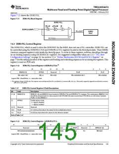
7.5.5 Main PLL Controller/SRIO/HyperLink/PCIe Clock Input Electrical Data/Timing
Table 7-26
Main PLL Controller/SRIO/HyperLink/PCIe Clock Input Timing Requirements (1) (Part 1 of 3)
(see Figure 7-19 and Figure 7-20)
No.
Min
Max Unit
CORECLK[P:N]
1
1
tc(CORCLKN)
tc(CORECLKP)
Cycle time _ CORECLKN cycle time
Cycle time _ CORECLKP cycle time
3.2
3.2
25
25
ns
ns
142
Peripheral Information and Electrical Specifications
Copyright 2012 Texas Instruments Incorporated

 TI [ TEXAS INSTRUMENTS ]