TMS320C6672
Multicore Fixed and Floating-Point Digital Signal Processor
SPRS708C—February 2012
www.ti.com
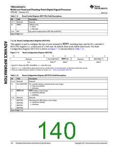
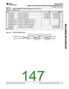
Table 7-26
Main PLL Controller/SRIO/HyperLink/PCIe Clock Input Timing Requirements (1) (Part 3 of 3)
(see Figure 7-19 and Figure 7-20)
No.
Min
Max Unit
1
1
3
2
2
3
4
4
4
4
5
5
tc(PCIECLKN)
Cycle time _ PCIECLKN cycle time
3.2
10
ns
ns
tc(PCIECLKP)
Cycle time _ PCIECLKP cycle time
3.2
10
tw(PCIECLKN)
Pulse width _ PCIECLKN high
0.45*tc(PCIECLKN)
0.55*tc(PCIECLKN)
ns
tw(PCIECLKN)
Pulse width _ PCIECLKN low
0.45*tc(PCIECLKN)
0.55*tc(PCIECLKN)
ns
tw(PCIECLKP)
Pulse width _ PCIECLKP high
0.45*tc(PCIECLKP)
0.55*tc(PCIECLKP)
ns
tw(PCIECLKP)
Pulse width _ PCIECLKP low
0.45*tc(PCIECLKP)
0.55*tc(PCIECLKP)
ns
tr(PCIECLKN_250mv)
tf(PCIECLKN_250mv)
tr(PCIECLKP_250mv)
tf(PCIECLKP_250mv)
tj(PCIECLKN)
Transition time _ PCIECLKN rise time (250 mV)
Transition time _ PCIECLKN fall time (250 mV)
Transition time _ PCIECLKP rise time (250 mV)
Transition time _ PCIECLKP fall time (250 mV)
Jitter, peak_to_peak _ periodic PCIECLKN
Jitter, peak_to_peak _ periodic PCIECLKP
50
50
50
50
350
350
350
350
4
ps
ps
ps
ps
ps,RMS
ps,RMS
tj(PCIECLKP)
4
End of Table 7-26
1 See the Hardware Design Guide for KeyStone devices in ‘‘Related Documentation from Texas Instruments’’ on page 69 for detailed recommendations.
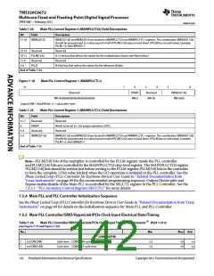
Figure 7-19
Figure 7-20
Main PLL Controller/SRIO/HyperLink/PCIe Clock Input Timing
1
2
3
5
<CLK_NAME>CLKN
<CLK_NAME>CLKP
4
Main PLL Clock Input Transition Time
peak-to-peak differential input
250 mV peak-to-peak
0
voltage (250 mV to 2 V)
TR = 50 ps min to 350 ps max (10% to 90 %)
for the 250 mV peak-to-peak centered at zero crossing
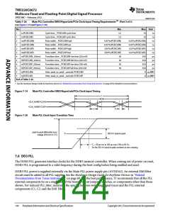
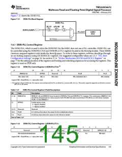
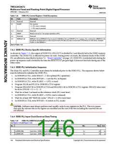
7.6 DD3 PLL
The DDR3 PLL generates interface clocks for the DDR3 memory controller. When coming out of power-on reset,
DDR3 PLL is programmed to a valid frequency during the boot config before being enabled and used.
DDR3 PLL power is supplied externally via the Main PLL power-supply pin (AVDDA2). An external EMI filter
circuit must be added to all PLL supplies. See the Hardware Design Guide for KeyStone Devices in ‘‘Related
Documentation from Texas Instruments’’ on page 69. For the best performance, TI recommends that all the PLL
external components be on a single side of the board without jumpers, switches, or components other than those
shown. For reduced PLL jitter, maximize the spacing between switching signal traces and the PLL external
components (C1, C2, and the EMI Filter).
144
Peripheral Information and Electrical Specifications
Copyright 2012 Texas Instruments Incorporated

 TI [ TEXAS INSTRUMENTS ]