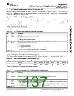
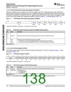
TMS320C6672
Multicore Fixed and Floating-Point Digital Signal Processor
SPRS708C—February 2012
www.ti.com
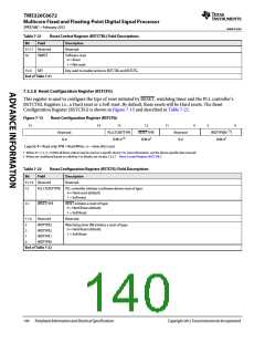
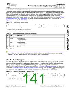
7.5.2.9 Reset Isolation Register (RSISO)
This register is used to select the module clocks that must maintain their clocking without pausing through non
power-on reset. Setting any of these bits effectively blocks reset to all PLLCTL registers in order to maintain current
values of PLL multiplier, divide ratios and other settings. Along with setting module specific bit in RSISO, the
corresponding MDCTLx[12] bit also needs to be set in PSC to reset isolate a particular module. For more
information on MDCTLx register see the Power Sleep Controller (PSC) for KeyStone Devices User Guide in ‘‘Related
Documentation from Texas Instruments’’ on page 69. The Reset Isolation Register (RSTCTRL) is shown in
Figure 7-16 and described in Table 7-23.
Figure 7-16
Reset Isolation Register (RSISO)
31
10
9
8
7
0
Reserved
R-0
SRIOISO
R/W-0
SRISO
R/W-0
Reserved
R-0
Legend: R = Read only; R/W = Read/Write; -n = value after reset
Table 7-23
Reset Isolation Register (RSISO) Field Descriptions
Bit
Field
Description
31-10 Reserved
Reserved.
9
SRIOISO
Isolate SRIO module
0 = Not reset isolated
1 = Reset Isolated
8
SRISO
Isolate SmartReflex
0 = Not reset isolated
1 = Reset Isolated
7-0
Reserved
Reserved.
End of Table 7-23
Note—The boot ROM code will enable the reset isolation for both SRIO and SmartReflex modules during
boot with the Reset Isolation Register. It is up to the user application to disable.
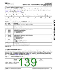
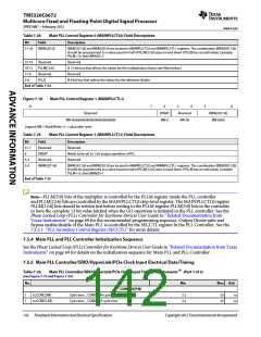
7.5.3 Main PLL Control Register
The Main PLL uses two chip-level registers (MAINPLLCTL0 and MAINPLLCTL1) along with the PLL controller
for its configuration. These MMRs exist inside the Bootcfg space. To write to these registers, software should go
through an un-locking sequence using KICK0/KICK1 registers. For valid configurable values into the
MAINPLLCTL0 and MAINPLLCTL1 registers see Section 2.5.3 ‘‘PLL Boot Configuration Settings’’ on page 34. See
section 3.3.4 ‘‘Kicker Mechanism (KICK0 and KICK1) Register’’ on page 77 for the address location of the registers
and locking and unlocking sequences for accessing the registers. The registers are reset on POR only.
Figure 7-17
Main PLL Control Register 0 (MAINPLLCTL0)
31
24
23
19
18
12
11
Reserved
RW-000000
6
5
0
BWADJ[7:0]
RW-0000 0101
Reserved
PLLM[12:6]
PLLD
RW-000000
RW-0000 0
RW-0000000
Legend: RW = Read/Write; -n = value after reset
Copyright 2012 Texas Instruments Incorporated
Peripheral Information and Electrical Specifications 141

 TI [ TEXAS INSTRUMENTS ]