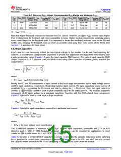
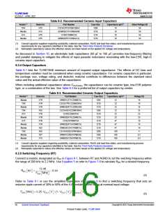
TLVM13640
SLVSGJ7 – APRIL 2022
www.ti.com
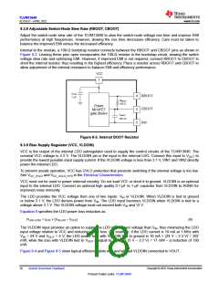
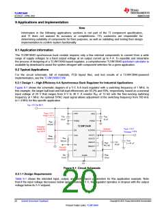
8.3.8 Adjustable Switch-Node Slew Rate (RBOOT, CBOOT)
Adjust the switch-node slew rate of the TLVM13640 to slow the switch-node voltage rise time and improve EMI
performance at high frequencies. However, slowing the rise time decreases efficiency. Care must be taken to
balance the improved EMI versus the decreased efficiency.
Internal to the module, a 100-Ω bootstrap resistor connects between the RBOOT and CBOOT pins as shown in
Figure 8-3. Leaving these pins open incorporates the 100-Ω resistor in the bootstrap circuit, slowing the switch
voltage slew rate and optimizing EMI. However, if improved EMI is not required, connect RBOOT to CBOOT to
short the internal resistor, thus resulting in the highest efficiency. Place a resistor across RBOOT and CBOOT to
allow adjustment of the internal resistance to balance EMI and efficiency performance.
VCC
7
CVCC
4
3
2
RBOOT
CBOOT
1 µF
RBOOT
100
Power
MOSFET
gate drivers
CBOOT
100 nF
SW
Figure 8-3. Internal BOOT Resistor
8.3.9 Bias Supply Regulator (VCC, VLDOIN)
VCC is the output of the internal LDO subregulator used to supply the control circuits of the TLVM13640. The
nominal VCC voltage is 3.3 V. The VLDOIN pin is the input to the internal LDO. Connect this input to VOUT to
provide the lowest possible input supply current. If the VLDOIN voltage is less than 3.1 V, VIN1 and VIN2 directly
power the internal LDO.
To prevent unsafe operation, VCC has UVLO protection that prevents switching if the internal voltage is too low.
See VCC_UVLO and VCC_UVLO_HYS in the Electrical Characteristics.
VCC must not be used to power external circuitry. Do not load VCC or short it to ground. VLDOIN is an optional
input to the internal LDO. Connect an optional high quality 0.1-µF to 1-µF capacitor from VLDOIN to AGND for
improved noise immunity.
The LDO provides the VCC voltage from one of two inputs: VIN or VLDOIN. When VLDOIN is tied to ground
or below 3.1 V, the LDO derives power from VIN. The LDO input becomes VLDOIN when VLDOIN is tied to a
voltage above 3.1 V. The VLDOIN voltage must not exceed both VIN and 12 V.
Equation 8 specifies the LDO power loss reduction as:
PLDO-LOSS = ILDO × (VIN-LDO – VVCC
)
(8)
The VLDOIN input provides an option to supply the LDO with a lower voltage than VIN, thus minimizing the LDO
input voltage relative to VCC and reducing power loss. For example, if the LDO current is 10 mA at 1 MHz with
VIN = 24 V and VOUT = 5 V, the LDO power loss with VLDOIN tied to ground is 10 mA × (24 V – 3.3 V) = 207
mW, while the loss with VLDOIN tied to VOUT is equal to 10 mA × (5 V – 3.3 V) = 17 mW – a reduction of 190
mW.
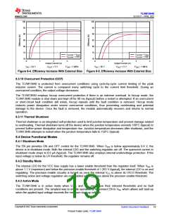
Figure 8-4 and Figure 8-5 show typical efficiency plots with and without VLDOIN connected to VOUT.
Copyright © 2022 Texas Instruments Incorporated
18
Submit Document Feedback
Product Folder Links: TLVM13640

 TI [ TEXAS INSTRUMENTS ]