TLVM13640
SLVSGJ7 – APRIL 2022
www.ti.com
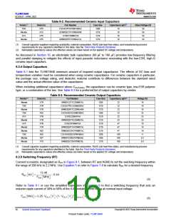
Table 8-1. Standard RFBT Values, Recommended FSW Range and Minimum COUT
VOUT RFBT (kΩ) Suggested FSW
COUT(min) (µF)
(Effective)
VOUT RFBT (kΩ) Suggested FSW
COUT(min) (µF)
(Effective)
CFF (pF)
CFF (pF)
(1)
(1)
(V)
Range (kHz)
300 to 500
400 to 600
500 to 700
(V)
2.5
3.3
5
Range (MHz)
650 to 900
700 to 950
0.8 to 1.2
1
Short
2
300
200
120
–
–
15
65
40
25
68
47
22
1.2
1.8
23.2
40.2
8.06
100
(1) RFBB = 10 kΩ
Note that higher feedback resistances consume less DC current. However, an upper RFBT resistor value higher
than 1 MΩ renders the feedback path more susceptible to noise. Higher feedback resistances generally require
more careful layout of the feedback path. It is important to locate the feedback resistors close to the FB and
AGND pins, keeping the feedback trace as short as possible (and away from noisy areas of the PCB). See
Section 11.2 guidelines for more detail.
8.3.3 Input Capacitors
Input capacitors are necessary to limit the input ripple voltage to the module due to switching frequency AC
currents. TI recommends using ceramic capacitors to provide low impedance and high RMS current rating over
a wide temperature range. Equation 2 gives the input capacitor RMS current. The highest input capacitor RMS
current occurs at D = 0.5, at which point, the RMS current rating of the capacitors should be greater than half the
output current.
DIL2
12
≈
’
D∂ IOUT2 ∂ 1-D +
∆
÷
÷
◊
ICIN,rms
=
(
)
∆
«
(2)
where
D = VOUT / VIN is the module duty cycle.
•
Ideally, the DC and AC components of input current to the buck stage are provided by the input voltage source
and the input capacitors, respectively. Neglecting inductor ripple current, the input capacitors source current of
amplitude (IOUT – IIN) during the D interval and sink IIN during the 1 – D interval. Thus, the input capacitors
conduct a square-wave current of peak-to-peak amplitude equal to the output current. The resultant capacitive
component of AC ripple voltage is a triangular waveform. Together with the ESR-related ripple component,
Equation 3 gives the peak-to-peak ripple voltage amplitude:
IOUT ∂D ∂ 1- D
(
)
+ IOUT ∂RESR
DV
=
IN
FSW ∂CIN
(3)
(4)
Equation 4 gives the input capacitance required for a particular load current:
D∂ 1-D ∂I
(
)
OUT
CIN
í
FSW ∂ DVIN -RESR ∂IOUT
where
ΔVIN is the input voltage ripple specification.
•
The TLVM13640 requires a minimum of two 10-µF ceramic input capacitors, preferably with X7R or X7S
dielectric and in 1206 or 1210 footprint. Additional capacitance can be required for applications to meet
conducted EMI specifications, such as CISPR 11 or CISPR 32.
Table 8-2 includes a preferred list of capacitors by vendor. To minimize the parasitic inductance in the switching
loops, position the ceramic input capacitors in a symmetrical layout close to the VIN1 and VIN2 pins and connect
the capacitor return terminals to the PGND pins using a copper ground plane under the module.
Copyright © 2022 Texas Instruments Incorporated
Submit Document Feedback
15
Product Folder Links: TLVM13640

 TI [ TEXAS INSTRUMENTS ]