TLVM13640
SLVSGJ7 – APRIL 2022
www.ti.com
8.3 Feature Description
8.3.1 Input Voltage Range (VIN1, VIN2)
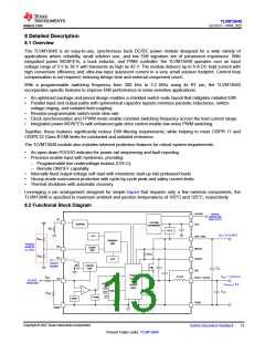
With a steady-state input voltage range from 3 V to 36 V, the TLVM13640 module is intended for step-down
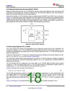
conversions from typical 12-V, 24-V, and 28-V input supply rails. The schematic circuit in Figure 8-1 shows all the
necessary components to implement a TLVM13640-based buck regulator using a single input supply.
VIN = 3 V to 36 V
VIN1
VIN2
CIN1
CIN2
PGND
PGND
RENT
TLVM13640
Precision enable
for VIN UVLO
Optional
external bias
VOUT = 1 V to 6 V
IOUT(max) = 4 A
EN
VLDOIN
VOUT
VOUT1
VOUT2
RENB
VCC
RPG
COUT
CBOOT
RBOOT
PG
RT
RFBT
PGOOD
indicator
FB
AGND
RRT
RFBB
Figure 8-1. TLVM13640 Schematic Diagram with Input Voltage Operating Range of 3 V to 36 V
The minimum input voltage required for start-up is 3.95 V. Take extra care to make sure that the voltage at the
VIN pins of the module (VIN1 and VIN2) does not exceed the absolute maximum voltage rating of 42 V during
line or load transient events. Voltage ringing at the VIN pins that exceeds the absolute maximum ratings can
damage the IC.
8.3.2 Adjustable Output Voltage (FB)
The TLVM13640 has an adjustable output voltage range from 1 V up to a maximum of 6 V or slightly less than
VIN, whichever is lower. Setting the output voltage requires two feedback resistors, designated as RFBT and RFBB
in Figure 8-1. The reference voltage at the FB pin is set at 1 V with a feedback system accuracy over the full
junction temperature range of ±1%. The junction temperature range for the device is –40°C to 125°C.
Calculate the value for RFBT using Equation 1 based on a recommended value for RFBB of 10 kΩ.
(1)
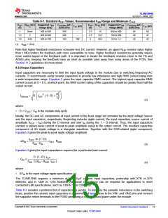
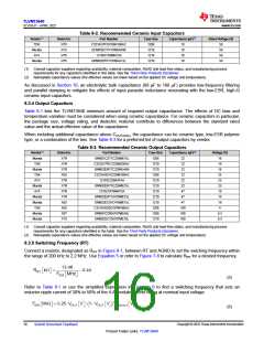
Table 8-1 lists the standard resistor values for several output voltages and the recommended switching
frequency range to maintain reasonable peak-to-peak inductor ripple current. This table also includes the
minimum required output capacitance for each output voltage setting to maintain stability. The capacitances
as listed represent effective values for ceramic capacitors derated for DC bias voltage and temperature.
Furthermore, place a feedforward capacitor, CFF, in parallel with RFBT to increase the phase margin when the
output capacitance is close to the minimum recommended value.
Copyright © 2022 Texas Instruments Incorporated
14
Submit Document Feedback
Product Folder Links: TLVM13640

 TI [ TEXAS INSTRUMENTS ]