TLVM13640
SLVSGJ7 – APRIL 2022
www.ti.com
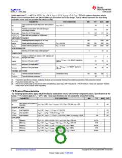
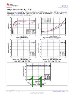
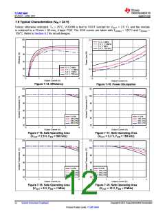
7.9 Typical Characteristics (VIN = 24 V)
Unless otherwise indicated, TA = 25°C, VLDOIN is tied to VOUT (except for VOUT = 2.5 V), and the module
is soldered to a 76-mm × 63-mm, 4-layer PCB. The SOA curves are taken with TJ(max) = 125°C and TA(max)
105°C. Refer to Section 9.2 for circuit designs.
=
100
95
90
85
80
75
2.5
12 V, 2 MHz
7.5 V, 1.5 MHz
5 V, 1 MHz
2
3.3 V, 750 kHz
1.5
1
12 V, 2 MHz
0.5
0
7.5 V, 1.5 MHz
5.0 V, 1 MHz
3.3 V, 750 kHz
0
1
2
3
4
0
1
2
3
4
Output Current (A)
Output Current (A)
Figure 7-14. Efficiency
Figure 7-15. Power Dissipation
120
100
80
60
0 LFM
40
100 LFM
200 LFM
400 LFM
20
0
1
2
3
4
Output Current (A)
Figure 7-16. Safe Operating Area
(VOUT = 2.5 V, FSW = 500 kHz)
Figure 7-17. Safe Operating Area
(VOUT = 3.3 V, FSW = 750 kHz)
120
100
80
120
100
80
60
60
0 LFM
0 LFM
40
40
100 LFM
200 LFM
400 LFM
100 LFM
200 LFM
400 LFM
20
20
0
1
2
3
4
0
1
2
3
4
Output Current (A)
Output Current (A)
Figure 7-18. Safe Operating Area
(VOUT = 5 V, FSW = 1 MHz)
Figure 7-19. Safe Operating Area
(VOUT = 12 V, FSW = 2 MHz)
Copyright © 2022 Texas Instruments Incorporated
12
Submit Document Feedback
Product Folder Links: TLVM13640

 TI [ TEXAS INSTRUMENTS ]