TLVM13640
SLVSGJ7 – APRIL 2022
www.ti.com
8 Detailed Description
8.1 Overview
The TLVM13640 is an easy-to-use, synchronous buck DC/DC power module designed for a wide variety of
applications where reliability, small solution size, and low EMI signature are of paramount importance. With
integrated power MOSFETs, a buck inductor, and PWM controller, the TLVM13640 operates over an input
voltage range of 3 V to 36 V with transients as high as 42 V. The module delivers up to 6-A DC load current with
high conversion efficiency and ultra-low input quiescent current in a very small solution footprint. Control loop
compensation is not required, reducing design time and external component count.
With a programmable switching frequency from 200 kHz to 2.2 MHz using its RT pin, the TLVM13640
incorporates specific features to improve EMI performance in noise-sensitive applications:
•
•
An optimized package and pinout design enables a shielded switch-node layout that mitigates radiated EMI.
Parallel input and output paths with symmetrical capacitor layouts minimize parasitic inductance, switch-
voltage ringing, and radiated field coupling
•
•
•
Resistor-programmable switch-node slew rate
Clock synchronization and FPWM mode enable constant switching frequency across the load current range.
Integrated power MOSFETs with enhanced gate drive control enable low-noise PWM switching.
Together, these features significantly reduce EMI filtering requirements, while helping to meet CISPR 11 and
CISPR 32 Class B EMI limits for conducted and radiated emissions.
The TLVM13640 module also includes inherent protection features for robust system requirements:
•
•
An open-drain PGOOD indicator for power-rail sequencing and fault reporting
Precision enable input with hysteresis, providing:
– Programmable line undervoltage lockout (UVLO)
– Remote ON/OFF capability
•
•
•
Internally fixed output-voltage soft start with monotonic start-up into prebiased loads
Hiccup-mode overcurrent protection with cycle-by-cycle peak and valley current limits
Thermal shutdown with automatic recovery.
Leveraging a pin arrangement designed for simple layout that requires only a few external components, the
TLVM13640 is specified to maximum ambient and junction temperatures of 105°C and 125°C, respectively.
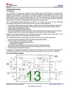
8.2 Functional Block Diagram
VLDOIN
VCC
Optional
external bias
(from VOUT)
RT
LDO bias
subregulator
VIN
Oscillator
RRT
UVLO
VIN = 3 V to 36 V
OTP
VIN1, VIN2
RENT
Shutdown
logic
Precision
enable for
VIN UVLO
EN
PG
Enable
logic
RBOOT
CBOOT
100 Ω
RENB
OCP
PGOOD
indicator
PGOOD
logic
CIN
SW
Power
stage
and
control
logic
2.2 µH
VOUT = 1 V to 6 V
IOUT(max) = 4 A
COUT
RFBT
VOUT1, VOUT2
FB
To VOUT
sense point
UVLO
OTP
OCP
EN
Soft start
+
RFBB
Comp
VREF
PGND
AGND
Copyright © 2022 Texas Instruments Incorporated
Submit Document Feedback
13
Product Folder Links: TLVM13640

 TI [ TEXAS INSTRUMENTS ]