TLK10002
www.ti.com
SLLSE75 –MAY 2011
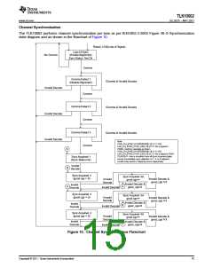
Low
Speed
Side
High
Speed
Side
HS_RXBCLK_A
INA [3:0]P/N
HSTXAP /N
VCO_CLOCK_A_DIV2
SERDES
SERDES
OUTA [3:0]P/N
HSRXAP /N
Channel A
Channel A
A S /W
2
Reg: 1.3:2
Reg: 1.7:4
_SEL
REFCLKA
4
Divide by N
+
_
CLKOUTAP/N
CLKOUTBP/N
(N= 1,2,4,5,8,
10,16,20,25)
+
_
0P/N
1P/N
REFCLK
REFCLK
Divide by N
+
_
+
_
,
(N= 1,2,4,5,8
10,16,20,25)
4
2
B S/W
_SEL
REFCLKB
Reg: 1.3:2
Reg: 1.7:4
Low
Speed
Side
High
Speed
Side
/N
HSTXBP
INB [3:0]P/N
VCO_CLOCK _B_DIV2
HS_RXBCLK_B
SERDES
Channel B
SERDES
Channel B
/N
HSRXBP
OUTB [3:0]P/N
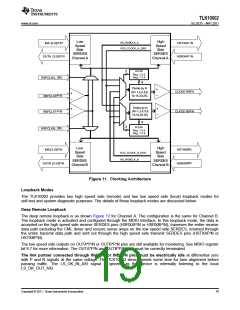
Figure 11. Clocking Architecture
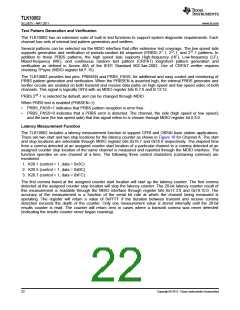
Loopback Modes
The TLK10002 provides two high speed side (remote) and two low speed side (local) loopback modes for
self-test and system diagnostic purposes. The details of those loopback modes are discussed below.
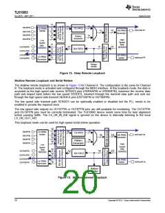
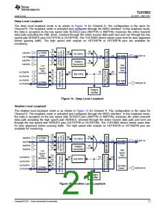
Deep Remote Loopback
The deep remote loopback is as shown Figure 12 for Channel A. The configuration is the same for Channel B.
The loopback mode is activated and configured through the MDIO interface. In this loopback mode, the data is
accepted on the high speed side receive SERDES pins (HSRXAP/N or HSRXBP/N), traverses the entire receive
data path excluding the CML driver and receive sense amps on the low speed side SERDES, returned through
the entire transmit data path and sent out through the high speed side transmit SERDES pins (HSTXAP/N or
HSTXBP/N).
The low speed side outputs on OUTA*P/N or OUTB*P/N pins are still available for monitoring. See MDIO register
bit 6.7 for more information. The OUTA*P/N and OUTB*P/N pins must be correctly terminated.
The link partner connected through INA*P/N or INB*P/N pins must be electrically idle at differential zero
with P and N signals at the same voltage. The TLK10002 device needs some time for lane alignment before
passing traffic. The LS_OK_IN_A/B signal is ignored as the device is internally listening to the local
LS_OK_OUT_A/B.
Copyright © 2011, Texas Instruments Incorporated
19

 TI [ TEXAS INSTRUMENTS ]