TLK10002
SLLSE75 –MAY 2011
www.ti.com
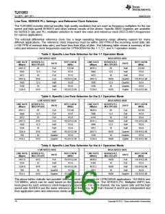
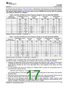
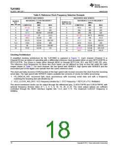
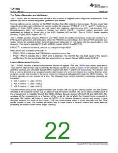
Table 8. Reference Clock Frequency Selection Example
LOW SPEED SIDE SERDES
HIGH SPEED SIDE SERDES
REFERENCE CLOCK FREQUENCY
(MHz)
REFERENCE CLOCK FREQUENCY
(MHz)
SERDES
PLL
MULTIPLIER
SERDES PLL
MULTIPLIER
COMPUTED
MIN
250
MAX
425
COMPUTED
742.5
594
MIN
375
MAX
425
4
5
371.25
297
4
5
200
425
300
425
6
247.5
185.625
148.5
123.75
118.8
99
166.667
125
416.667
312.5
250
6
495
250
425
8
8
371.25
297
187.5
150
390.625
312.5
10
12
12.5
15
20
122.88
122.88
122.88
122.88
122.88
10
12
12.5
15
16
20
208.333
200
247.5
237.6
198
125
260.417
250
153.6
122.88
122.88
122.88
166.667
125
208.333
195.3125
156.25
74.25
185.625
148.5
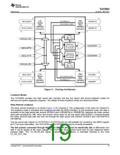
Clocking Architecture
A simplified clocking architecture for the TLK10002 is captured in Figure 11. Each channel (Channel A or
Channel B) has an option of operating with a differential reference clock provided either on pins REFCLK0P/N or
REFCLK1P/N. The choice is made either through MDIO or through REFCLKA_SEL and REFCLKB_SEL pins.
The reference clock frequencies for those two clock inputs can be different as long as they fall under the valid
ranges shown in Table 7. For each channel, the low speed side SERDES, high speed side SERDES and the
associated part of the digital core operate from the same reference clock.
The clock and data recovery (CDR) function of the high speed side receiver recovers the clock from the incoming
serial data. The high speed side SERDES makes available two versions of clocks for further processing:
1. HS_RXBCLK_A/B: recovered byte clock synchronous with incoming serial data and with a frequency
matching the incoming line rate divided by 20.
2. VCO_CLOCK_A/B_DIV2: VCO frequency divided by 2. (VCO frequency = REFCLK x PLL Multiplier).
The above-mentioned clocks can be output through the differential pins, CLKOUTAP/N and CLKOUTBP/N, with
optional frequency division ratios of 1, 2, 4, 5, 8, 10, 16, 20, or 25. The clock output options are software
controlled through the MDIO interface register bits 1.3:2, and 1.7:4. The maximum CLKOUT frequency is
500MHz.
18
Copyright © 2011, Texas Instruments Incorporated

 TI [ TEXAS INSTRUMENTS ]