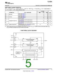
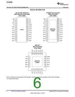
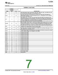
TLC5928
www.ti.com ................................................................................................................................................. SBVS120A–JULY 2008–REVISED SEPTEMBER 2008
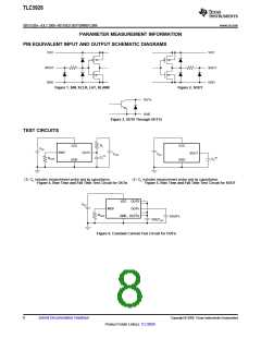
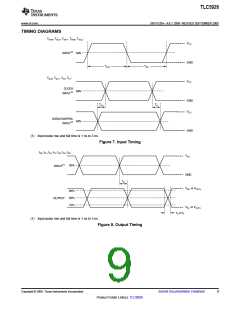
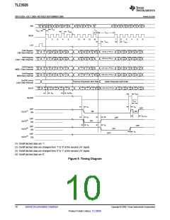
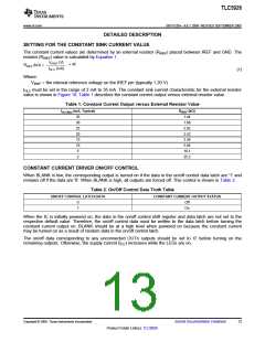
TIMING DIAGRAMS
TWH0, TWL0, TWH1, TWH2, TWL2
:
VCC
INPUT(1) 50%
GND
TWH
TWL
TSU0, TSU1, TH0, TH1
:
VCC
CLOCK
INPUT(1)
50%
GND
VCC
TSU
TH
DATA/CONTROL
INPUT(1)
50%
GND
(1) Input pulse rise and fall time is 1 ns to 3 ns.
Figure 7. Input Timing
tR0, tR1, tF0, tF1, tD0, tD1, tD2
:
VCC
INPUT(1)
50%
GND
tD
VOH or VOUTn
90%
50%
10%
OUTPUT
VOL or VOUTn
tR or tF
(1) Input pulse rise and fall time is 1 ns to 3 ns.
Figure 8. Output Timing
Copyright © 2008, Texas Instruments Incorporated
Submit Documentation Feedback
9
Product Folder Link(s): TLC5928

 TI [ TEXAS INSTRUMENTS ]