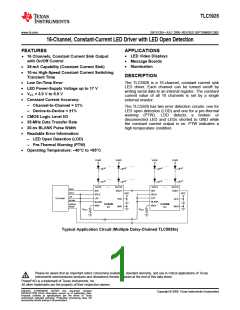
TLC5928
www.ti.com ................................................................................................................................................. SBVS120A–JULY 2008–REVISED SEPTEMBER 2008
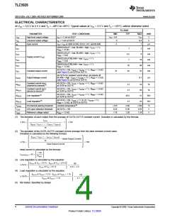
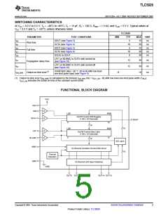
SWITCHING CHARACTERISTICS
At VCC = 3.0 V to 5.5 V, TA = –40°C to +85°C, CL = 15 pF, RL = 130 Ω, RIREF = 1.5 kΩ, and VLED = 5.5 V. Typical values at
VCC = 3.3 V and TA = +25°C, unless otherwise noted.
TLC5928
PARAMETER
TEST CONDITIONS
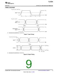
SOUT (see Figure 5)
MIN
TYP
5
MAX
15
UNIT
ns
tR0
tR1
tF0
tF1
tD0
Rise time
OUTn (see Figure 4)
SOUT (see Figure 5)
OUTn (see Figure 4)
SCLK↑ to SOUT
10
5
30
ns
15
ns
Fall time
10
8
30
ns
20
ns
LAT↑ or BLANK↓ to OUTn sink current on
(see Figure 10)
tD1
12
12
30
30
+8
ns
ns
ns
Propagation delay time
Output on-time error(1)
LAT↑ or BLANK↑ to OUTn sink current off
(see Figure 10)
tD2
On/off latch data = all '1', 20 ns BLANK low level
one-shot pulse input (see Figure 4)
tON_ERR
–8
(1) Output on-time error (tON_ERR) is calculated by the formula: tON_ERR (ns) = tOUT_ON – BLANK low level one-shot pulse width (TWL2).
tOUT_ON indicates the actual on-time of the constant current driver.
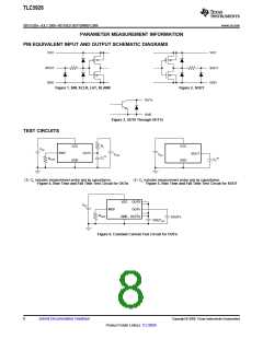
FUNCTIONAL BLOCK DIAGRAM
VCC
VCC
SIN
LSB
MSB
On/Off Control Shift Register
(1 Bit x 16 Channels)
SCLK
SOUT
0
15
16
16
MSB
LSB
LAT
On/Off Control Data Latch
(1 Bit x 16 Channels)
0
15
BLANK
16
SID Latch
IREF
GND
16-Channel Constant Current Sink Driver
16
Thermal
Detection
16-Channel LED Open Detection
GND
¼
OUT0 OUT1
OUT14 OUT15
Copyright © 2008, Texas Instruments Incorporated
Submit Documentation Feedback
5
Product Folder Link(s): TLC5928

 TI [ TEXAS INSTRUMENTS ]