TLC5928
SBVS120A–JULY 2008–REVISED SEPTEMBER 2008 ................................................................................................................................................. www.ti.com
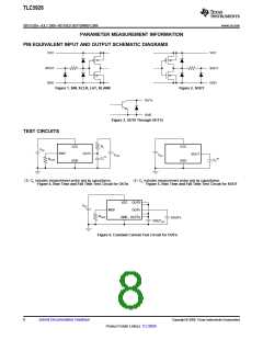
PARAMETER MEASUREMENT INFORMATION
PIN EQUIVALENT INPUT AND OUTPUT SCHEMATIC DIAGRAMS
VCC
VCC
INPUT
GND
SOUT
GND
Figure 1. SIN, SCLK, LAT, BLANK
Figure 2. SOUT
OUTn
GND
Figure 3. OUT0 Through OUT15
TEST CIRCUITS
RL
CL
VCC
GND
VCC
VCC
IREF
OUTn
SOUT
GND
VLED
VCC
(1)
(1)
CL
RIREF
(1) CL includes measurement probe and jig capacitance.
(1) CL includes measurement probe and jig capacitance.
Figure 4. Rise Time and Fall Time Test Circuit for OUTn
Figure 5. Rise Time and Fall Time Test Circuit for SOUT
VCC
OUT0
OUTn
VCC
IREF
RIREF
GND OUT15
VOUTn
VOUTFIX
Figure 6. Constant Current Test Circuit for OUTn
8
Submit Documentation Feedback
Copyright © 2008, Texas Instruments Incorporated
Product Folder Link(s): TLC5928

 TI [ TEXAS INSTRUMENTS ]