TLC5928
www.ti.com ................................................................................................................................................. SBVS120A–JULY 2008–REVISED SEPTEMBER 2008
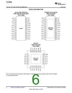
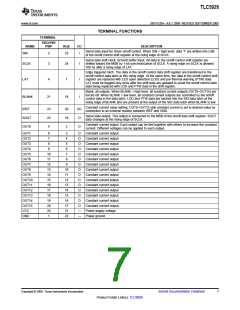
TERMINAL FUNCTIONS
TERMINAL
DBQ/PW/
NAME
SIN
PWP
RGE
I/O
DESCRIPTION
Serial data input for driver on/off control. When SIN = high level, data '1' are written into LSB
of the on/off control shift register at the rising edge of SCLK.
2
23
I
Serial data shift clock. Schmitt buffer input. All data in the on/off control shift register are
shifted toward the MSB by 1-bit synchronization of SCLK. A rising edge on SCLK is allowed
100 ns after a rising edge of LAT.
SCLK
LAT
3
4
24
1
I
I
Edge triggered latch. The data in the on/off control data shift register are transferred to the
on/off control data latch at this rising edge. At the same time, the data in the on/off control shift
register are replaced with LED open detection (LOD) and pre-thermal warning (PTW) data.
LAT must be toggled only once after the shift data are updated to avoid the on/off control latch
data being replaced with LOD and PTW data in the shift register.
Blank, all outputs. When BLANK = high level, all constant current outputs (OUT0–OUT15) are
forced off. When BLANK = low level, all constant current outputs are controlled by the on/off
control data in the data latch. LOD and PTW data are latched into the SID data latch at the
rising edge of BLANK and are present at the output of the SID data latch when BLANK is low.
BLANK
21
18
I
Constant current value setting, OUT0–OUT15 sink constant current is set to desired value by
connection to an external resistor between IREF and GND.
IREF
23
22
5
20
19
2
I/O
O
Serial data output. This output is connected to the MSB of the on/off data shift register. SOUT
data changes at the rising edge of SCLK.
SOUT
OUT0
Constant current output. Each output can be tied together with others to increase the constant
current. Different voltages can be applied to each output.
O
OUT1
OUT2
OUT3
OUT4
OUT5
OUT6
OUT7
OUT8
OUT9
OUT10
OUT11
OUT12
OUT13
OUT14
OUT15
VCC
6
3
4
O
O
O
O
O
O
O
O
O
O
O
O
O
O
O
—
—
Constant current output
Constant current output
Constant current output
Constant current output
Constant current output
Constant current output
Constant current output
Constant current output
Constant current output
Constant current output
Constant current output
Constant current output
Constant current output
Constant current output
Constant current output
Power-supply voltage
Power ground
7
8
5
9
6
10
11
12
13
14
15
16
17
18
19
20
24
1
7
8
9
10
11
12
13
14
15
16
17
21
22
GND
Copyright © 2008, Texas Instruments Incorporated
Submit Documentation Feedback
7
Product Folder Link(s): TLC5928

 TI [ TEXAS INSTRUMENTS ]