SN65HVS883
www.ti.com.cn
ZHCSFI0 –SEPTEMBER 2016
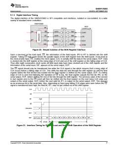
9.1.3 Digital Interface Timing
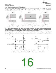
The digital interface of the SN65HVS883 is SPI compatible and interfaces, isolated or non-isolated, to a wide
variety of standard micro controllers.
SN65HVS883
HOST
SIP
ISO7241
CONTROLLER
IP0
IP7
LD
CE
OUTA
OUTB
OUTC
IND
INA
INB
LOAD
STE
CLK
SOP
INC
SCLK
SOMI
OUTD
Figure 20. Simple Isolation of the Shift Register Interface
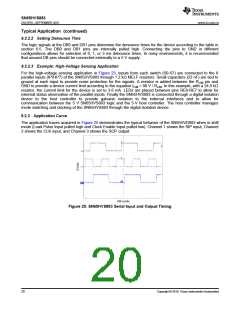
Upon a low-level at the load input, LD, the information of the field inputs, IP0 to IP7 is latched into the shift
register. Taking LD high again blocks the parallel inputs of the shift register from the field inputs. A low-level at
the clock-enable input, CE, enables the clock signal, CLK, to serially shift the data to the serial output, SOP. Data
is clocked into the shift register at the rising edge of CLK and out of the shift register on the falling edge of CLK.
Thus after eight consecutive clock cycles all field input data have been clocked out of the shift register and the
information of the serial input, SIP, appears at the serial output, SOP.
The CE signal should only be transitioned low while the CLK signal is low which ensures that a rising edge of
CLK occurs before a falling edge of CLK. This shifts the data into and through the shift register up until the final
register before the first bit that was loaded into the final register is shifted out the serial output, SOP. If a falling
edge of CLK is seen first following the transition of CE to low, the final register outputs the first bit, IP0, on the
serial output, SOP, before shifting the rest of the bits through the shift register. The previous value of the second
to last register prior to the LD event will then be shifted into the final register on the next rising CLK edge and
output on the serial output, SOP, before the next valid bit, IP1, is output on the serial output, SOP. This appears
as an erroneous bit in the serial data. Also, depending on how many falling CLK edges were seen before the CE
signal is transitioned back high, the final bit, IP7, may not get shifted out of the shift register.
CLK
CE
SIP
high
LD
PIP0-PIP6
PIP7
SOP
IP7
Inhibit
IP6
IP5
IP4
IP3
IP2
IP1
IP0
SIP
don’t care
Serial shift
Figure 21. Interface Timing for Parallel-Load and Serial-Shift Operation of the Shift Register
Copyright © 2016, Texas Instruments Incorporated
17

 TI [ TEXAS INSTRUMENTS ]