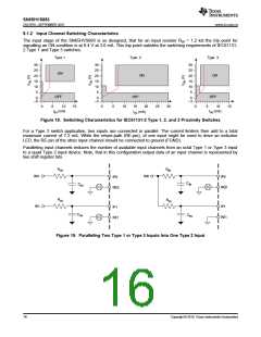
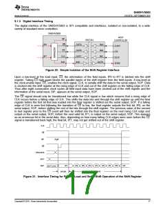
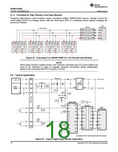
SN65HVS883
ZHCSFI0 –SEPTEMBER 2016
www.ti.com.cn
Typical Application (continued)
9.2.2.2 Setting Debounce Time
The logic signals at the DB0 and DB1 pins determine the denounce times for the device according to the table in
section 6.5. The DB0 and DB1 pins are internally pulled high. Connecting the pins to GND in different
configurations allows for selection of 0, 1, or 3 ms debounce times. In noisy environments, it is recommended
that unused DB pins should be connected externally to a 5 V supply.
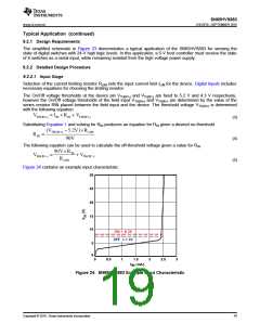
9.2.2.3 Example: High-Voltage Sensing Application
For the high-voltage sensing application in Figure 23, inputs from each switch (S0-S7) are connected to the 8
parallel inputs (IP0-IP7) of the SN65HVS883 through 1.2 kΩ MELF resistors. Small capacitors (22 nF) are tied to
ground at each input to provide noise protection for the signals. A resistor is added between the RLIM pin and
GND to provide a device current limit according to the equation ILIM = 90 V / RLIM. In this example, with a 24.9 kΩ
resistor, the current limit for the device is set to 3.6 mA. LEDs are placed between pins RE0-RE7 to allow for
external status observation of the parallel inputs. Finally the SN65HVS883 is connected through a digital isolation
device to the host controller to provide galvanic isolation to the external interfaces and to allow for
communication between the 5 V SN65HVS883 logic and the 5-V host controller. The host controller manages
mode switching and clocking of the SN65HVS883 through the digital isolation device.
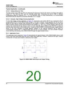
9.2.3 Application Curve
The application traces acquired in Figure 25 demonstrates the typical behavior of the SN65HVD883 when in shift
mode (Load Pulse Input pulled high and Clock Enable Input pulled low). Channel 1 shows the SIP input, Channel
2 shows the CLK input, and Channel 3 shows the SOP output.
500 ns/div
Figure 25. SN65HVS883 Serial Input and Output Timing
20
Copyright © 2016, Texas Instruments Incorporated

 TI [ TEXAS INSTRUMENTS ]