SN65HVS883
www.ti.com.cn
ZHCSFI0 –SEPTEMBER 2016
10 Power Supply Recommendations
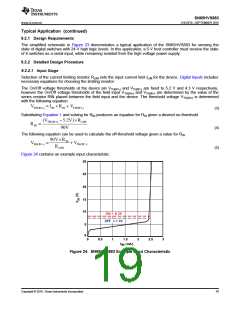
The SN65HVS883 operates within a recommended supply voltage range from 4.5 V to 5.5 V. A 0.1 µF or larger
capacitor should be placed between VCC and ground to improve power supply noise immunity. A current limiting
resistor can be used to reduce overall power consumption as described in Digital Inputs. The high voltage
parallel field inputs can accept voltages ranging from 0 V to 34 V, however all other inputs must remain between
0 V to 5 V. Refer to the Recommended Operating Conditions table for more detailed voltage suggestions. High
voltage field inputs should be buffered as shown in Figure 23 to improve input noise immunity.
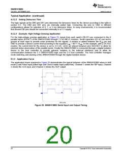
11 Layout
11.1 Layout Guidelines
1. Place series MELF resistors between the field inputs and the device input pins.
2. Place small ~22 nF capacitors close to the field input pins to reduce noise.
3. Place a supply buffering 0.1-µF capacitor around as close to the VCC pin as possible.
11.2 Layout Example
1
R
2
C
R
R
R
C
C
C
High
{b65Iëꢀ883
Voltage
Parallel
Inputs
Isolator
MCU
R
R
R
R
C
C
C
C
R
C
C
3
Isolated
DC-DC
Via to ground
Via to VCC 5V
Via to VCC 24V
版权 © 2016, Texas Instruments Incorporated
21

 TI [ TEXAS INSTRUMENTS ]