SN65HVS883
ZHCSFI0 –SEPTEMBER 2016
www.ti.com.cn
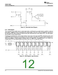
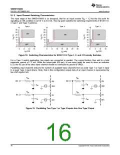
9.1.2 Input Channel Switching Characteristics
The input stage of the SN65HVS883 is so designed, that for an input resistor RIN = 1.2 kΩ the trip point for
signalling an ON-condition is at 9.4 V at 3.6 mA. This trip point satisfies the switching requirements of IEC61131-
2 Type 1 and Type 3 switches.
Type 1
Type 2
Type 3
30
25
20
15
10
5
30
25
20
15
10
5
30
25
20
15
10
5
ON
ON
ON
OFF
10
OFF
15
OFF
0
–3-
0
–3
0
–3
5
15
5
10
20
(mA)
25
30
5
10
(mA)
15
0
0
0
I
(mA)
I
IN
I
IN
IN
Figure 18. Switching Characteristics for IEC61131-2 Type 1, 2, and 3 Proximity Switches
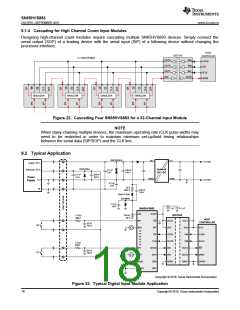
For a Type 2 switch application, two inputs are connected in parallel. The current limiters then add to a total
maximum current of 7.2 mA. While the return-path (RE-pin), of one input might be used to drive an indicator
LED, the RE-pin of the other input channel should be connected to ground (FGND).
Paralleling input channels reduces the number of available input channels from an octal Type 1 or Type 3 input
to a quad Type 2 input device. Note, that in this configuration output data of an input channel is represented by
two shift register bits.
R
R
IN
IN
IN0
IN0
IP0
IP0
C
C
IN
IN
RE0
RE0
R
R
IN
IN
IN1
IP1
IP1
C
C
IN
IN
RE1
RE1
Figure 19. Paralleling Two Type 1 or Type 3 Inputs Into One Type 2 Input
16
Copyright © 2016, Texas Instruments Incorporated

 TI [ TEXAS INSTRUMENTS ]