SN65HVS883
ZHCSFI0 –SEPTEMBER 2016
www.ti.com.cn
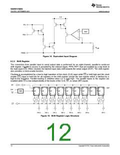
5 V
IPx
REF
REx
R
LIM
FGND
Figure 14. Equivalent Input Diagram
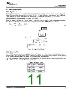
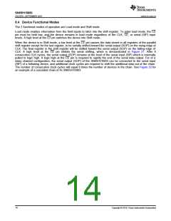
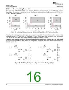
8.3.3 Shift Register
The conversion from parallel input to serial output data is performed by an eight-channel, parallel-in serial-out
shift register. Parallel-in access is provided by the internal inputs, PIP0–PIP7, that are enabled by a low level at
the load input (LD). When clocked, the latched input data shift towards the serial output (SOP). The shift register
also provides a clock-enable function.
Clocking is accomplished by a low-to-high transition of the clock (CLK) input while LD is held high and the clock
enable (CE) input is held low for all registers in the shift register except the last register which is latched by a
high-to-low transition. Parallel loading is inhibited when LD is held high. The parallel inputs to the register are
enabled while LD is low independently of the levels of the CLK, CE, or serial (SIP) inputs.
SIP
SOP
D
D
D
D
D
D
D
D
D
Q
S
Q
S
Q
S
Q
S
Q
S
Q
S
Q
S
Q
Q
S
CLK
CE
Logic
CP
R
CP
R
CP
R
CP
R
CP
R
CP
R
CP
R
CP
CP
R
LD
PIP 0
PIP 1
PIP 2
PIP 3
PIP 4
PIP 5
PIP 6
PIP 7
Figure 15. Shift Register Logic Structure
12
Copyright © 2016, Texas Instruments Incorporated

 TI [ TEXAS INSTRUMENTS ]