PGA400-Q1
SLDS186 –MARCH 2012
www.ti.com
6.4.2 ICAP Supply for Capacitive Sensors
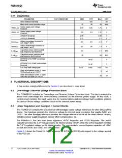
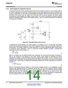
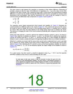
A functional schematic of the capacitive sensor drive circuit is shown in Figure 6-2. The common node of
the sensor capacitances is tied to the ICAP pin and the current and voltage at this point are referred to as
IX and VX respectively. For the sake of understanding the operation of the drive circuit by itself, the other
terminals of the sensor may be treated as if they were tied to ground, because the sensor signal
measurement circuit regulates the voltage at these nodes. This circuit is essentially a relaxation oscillator
where the capacitance of the sensor, the charging current IC, and the comparator hysteresis VH determine
the frequency of oscillation.
AVDD
I
C
S
1
ICAP
I
x
V
x
R
+
S
V
2
Sensor
H
_
I
R
C
A
C
C
B
Figure 6-2. Capacitive Sensor Drive Circuit
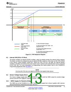
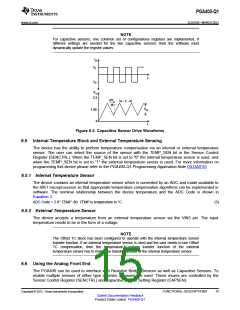
To illustrate the circuit operation, the sensor voltage VX is initially set to 0 V. In this state, the positive
terminal of the hysteretic comparator is lower than its negative reference terminal, producing a logical zero
at the output. This results is switch S2 is open and switch S1 is closed, allowing the upper current source
to charge the sensor capacitance. Figure 6-3 shows the resulting waveform. Equation 1 calculates the
linear ramp up slope of the voltage, VX:
dVx
1C
=
dt CA+CB
(1)
After VX is charged up to the high threshold of the comparator, the circuit inverts the states of switches S1
and S2. By closing S2 and opening S1 the lower current source begins to discharge the sensor
capacitances, making VX ramp down with an equal but opposite rate as before. Once VX reaches the low
threshold of the comparator, the circuit again inverts the states of the switches and returns to the positive
charging state. This process of charging and discharging repeats with a period characterized as shown in
Equation 2.
2•VH
T =
•(CA+CB)
IC
(2)
Both the comparator hysteresis voltage VH and capacitor charging current IC are configurable to allow
control of the oscillation period for a particular sensor. Bits CV[1..0] in the Capacitive Sensor Settings
Register (CAPSEN) can be used to set VH. VH can be set between 100 mV and 700 mV with four possible
steps. Bits CI[2..0] in the Capacitive Sensor Settings Register (CAPSEN) can be used to set IC, with
possible values between 5 µA and 22 µA with eight possible steps. For more information on programming
this device please refer to the PGA400-Q1 Programming Application Note (SLDA015)
14
FUNCTIONAL DESCRIPTIONS
Copyright © 2012, Texas Instruments Incorporated
Submit Documentation Feedback
Product Folder Link(s): PGA400-Q1

 TI [ TEXAS INSTRUMENTS ]