PGA400-Q1
www.ti.com
SLDS186 –MARCH 2012
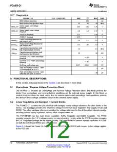
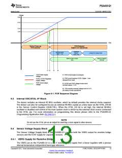
Voltage
5.0V
4.5V
3.3V
2.8V
time
Device Power-up
POR asserted
POR Released
Digital Core Operational
EEPROM
Bank 6
Load = 8us
EEPROM WAIT
Cycle = 12us
Analog Trim Values Valid
M8051w Held in Reset
30us
M8051w Program
Running
t1 t2
t3
t4
VDD Power supply
voltage
t1: POR circuit begins to energize
t2: POR circuit reaches DVDD, Digital Core
released from reset
AVDD, DVDD Regulator
supply voltage
POR Circuit output
voltage
t3: DVDD and POR voltage levels reach
nominal values = 3.3V
t4: VDD reaches nominal voltage level of 4.5V,
all analog circuits operational
Figure 6-1. POR Sequence Diagram
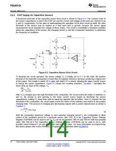
6.3 Internal OSC/XTAL I/F Block
The device includes an internal 40 MHz oscillator, which by default provides the internal clocks required.
The device can also be configured to use an external 40-MHz crystal as a time base via the XTAL_EN bit
in the Sensor Control Register (SENCTRL). When the XTAL_EN bit is set high, the internal 40-MHz
oscillator is disabled and control of the main system clock is driven by the external clock source connected
to the XTAL pin. For more information on programming this device please refer to the PGA400-Q1
Programming Application Note (SLDA015).).
NOTE
Do not use the XTAL pin as an output for sourcing a clock signal to other devices.
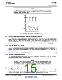
6.4 Sensor Voltage Supply Block
The Sensor Voltage Supply block of the PGA400-Q1 supplies both the VBRG output for resistive bridge
sensors and the ICAP supply for capacitive sensors.
6.4.1 VBRG Supply for Resistive Bridges
The VBRG pin on the PGA400-Q1 is a 3.3-V nominal output supply from a linear regulator with a precise
internal temperature independent band-gap reference.
Copyright © 2012, Texas Instruments Incorporated
FUNCTIONAL DESCRIPTIONS
13
Submit Documentation Feedback
Product Folder Link(s): PGA400-Q1

 TI [ TEXAS INSTRUMENTS ]